EZ-PD™ CCG7D Automotive USB Type-C and Buck-boost Controller
Dual-port
Applications
5
Applications
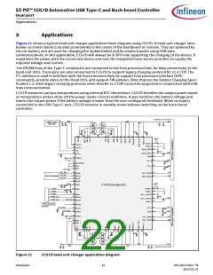
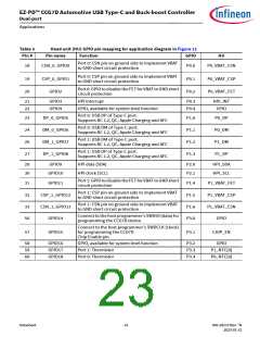
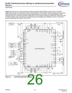
Figure 11 shows a typical head unit charger application block diagram using CCG7D. A head unit charger (also
known as center stack) is located prominently in the center of the dashboard or console. They are powered by
the car battery and are used for charging the mobile/tablet and for media transfer using USB data
communications. In this application, CCG7D will always be in DFP role supporting the charging of the device. It
negotiates the power with the connected device and uses the integrated buck-boost controller to supply the
required voltage and current.
The DP/DM lines of the Type-C receptacles are connected to the host processor/hub, for data connectivity to the
head unit (HU). These pins are also connected to CCG7D to support legacy charging protocol BC v1.2 CDP. The
I2C interface is used to interface with the host processor/hub, to support host processor interface (HPI)
commands, provide status to the Head Unit, and support FW updates. Note that per the Battery Charging Speci-
fication 1.2, other legacy charging protocols other than BC v1.2 CDP cannot be supported in conjunction with USB
data communication.
CCG7D measures various temperatures using external NTC thermistors. CCG7D throttles the output power based
on temperature and/or shuts off the power under critical conditions. It also monitors the battery voltage and
lowers the output power if the battery voltage is lower than the user-configured threshold. When no load is
connected to the USB Type-C port, CCG7D remains in standby mode without switching on the buck-boost
controller.
(USB PD, 3.3-21V, 5A)
5 m
5 m
VIN
VBUS
Battery Input
(9V-18V)
VDDD
VDDD
0.1μF
0.1μF
68
67
1
2
5
9
7
8
6
11 12
13
17
14
VDDD
1μF
4
3
PVDD_0
PGND_0
66
CSNI_0
65
61
62
CSPI_0
VIN
18
CSN_0_GPIO0
5 m
19
20
GND
CC1
CSP_0_GPIO1
GPIO2
VCCD
0.1μF
10
COMP_0
15
16
CC1_0
CC2_0
390pF
69
64
34
GND (EPAD)
CC2
390pF
GND
GND
AGND
HPI_SDA
HPI_SCL
HPI_INT
DP
29
30
21
22
23
24
DP_0_GPIO5
DM_0_GPIO6
GPIO9
GPIO10
GPIO3
GPIO4
DM
Host Processor
VDDD
63
25
VDDD
VDDD
VDDD
CYPD7291-68LDXS
0.1μF
10μF
1μF
48
49
VDDD
AGND
1
2
3
4
PVDD_1
PGND_1
0.1μF 1μF
33
XRES
28
57
XRES
CSN_1_GPIO13
5 m
SWD_CLK
GPIO15
32
31
GND
CSP_1_GPIO12
GPIO11
SWD_DAT
CHIP_EN
56
58
5
GPIO14
GPIO16
Programming Header
– not needed for final
production
CC1
CC2
37
36
P1_NTC[0]
59
60
CC1_1
CC2_1
GPIO17
GPIO18
390pF
390pF
P0_NTC[0]
42
COMP_1
27
26
DP
DP_1_GPIO8
DM_1_GPIO7
DM
55
54
CSPI_1
CSNI_1
52
53 51 50
47 43
45 44 46 41 40
VDDD
39
35
38
VDDD
0.1μF
0.1μF
VBUS
VIN
5 m
5 m
(USB PD, 3.3-21V, 5A)
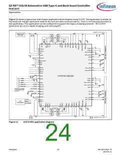
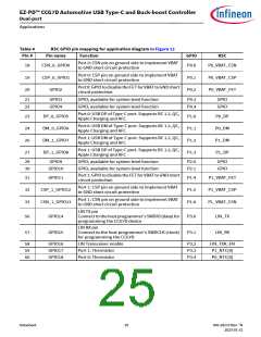
Figure 11
CCG7D head unit charger application diagram
Datasheet
22
002-28172 Rev. *N
2023-01-31

 INFINEON [ Infineon ]