EZ-PD™ CCG7D Automotive USB Type-C and Buck-boost Controller
Dual-port
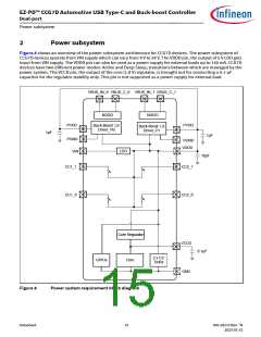
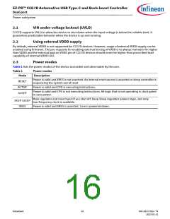
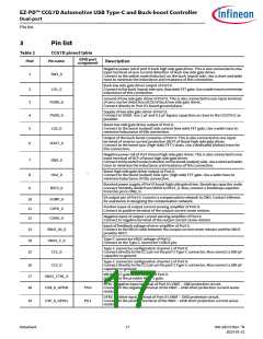
Functional overview
1.8
System resources
1.8.1
Watchdog timer (WDT)
CCG7D devices have a watchdog timer running from the internal low-speed oscillator (ILO). This allows watchdog
operation during Deep Sleep and generate a watchdog reset if not serviced before the timeout occurs. The
watchdog reset is recorded in the Reset Cause register.
1.8.2
Reset
CCG7D devices can be reset from a variety of sources including a Software Reset. Reset events are asynchronous
and guarantee reversion to a known state. The Reset cause is recorded in a Register, which is sticky through Reset
and allows software to determine the cause of the reset. XRES pin is the dedicated pin for reset to apply hardware
reset.
1.8.3
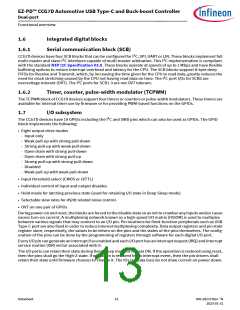
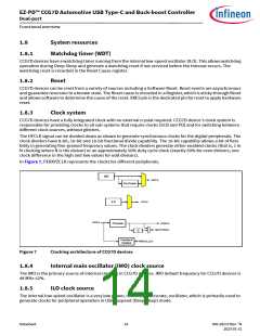
Clock system
CCG7D devices have a fully integrated clock with no external crystal required. CCG7D device’s clock system is
responsible for providing clocks to all sub-systems that require clocks (SCB and PD) and for switching between
different clock sources, without glitches.
The HFCLK signal can be divided down as shown to generate synchronous clocks for the digital peripherals. The
clock dividers have 8-bit, 16-bit and 16-bit fractional divide capability. The 16-bit capability allows a lot of flexi-
bility in generating fine-grained frequency values. The clock dividers generate either enabled clocks (that is, 1 in
N clocking where N is the divisor) or an approximately 50% duty cycle clock (exactly 50% for even divisors, one
clock difference in the high and low values for odd divisors).
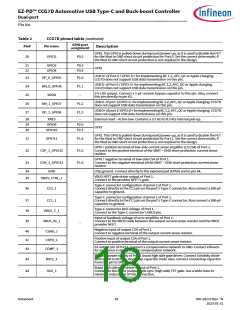
In Figure 7, PERXYZCLK represents the clocks for different peripherals.
IMO
HFCLK
Pre-Divider
ILO
LFCLK
HFCLK
Prescaler
SYSCLK
HALFSYSCLK
/2
Peripheral
Dividers
PERXYZ_CLK
Figure 7
Clocking architecture of CCG7D devices
1.8.4
Internal main oscillator (IMO) clock source
The IMO is the primary source of internal clocking in CCG7D devices. IMO default frequency for CCG7D devices is
48 MHz 2%.
1.8.5
ILO clock source
The internal low-speed oscillator is a very low power, relatively inaccurate, oscillator, which is primarily used to
generate clocks for peripheral operation in USB suspend (Deep Sleep) mode.
Datasheet
14
002-28172 Rev. *N
2023-01-31

 INFINEON [ Infineon ]