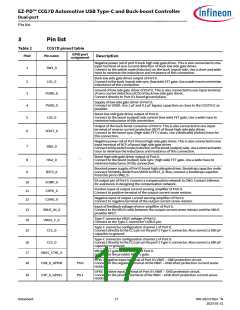
EZ-PD™ CCG7D Automotive USB Type-C and Buck-boost Controller
Dual-port
Functional overview
1.6
Integrated digital blocks
1.6.1
Serial communication block (SCB)
CCG7D devices have four SCB blocks that can be configured for I2C, SPI, UART or LIN. These blocks implement full
multi-master and slave I2C interfaces capable of multi-master arbitration. This I2C implementation is compliant
with the standard NXP I2C Specification V3.0. These blocks operate at speeds of up to 1 Mbps and have flexible
buffering options to reduce interrupt overhead and latency for the CPU. The SCB blocks support 8-byte deep
FIFOs for Receive and Transmit, which, by increasing the time given for the CPU to read data, greatly reduces the
need for clock stretching caused by the CPU not having read data on time. The I2C port I/Os for SCB0 are
overvoltage tolerant (OVT). The I2C ports for SCB1-3 are not OVT tolerant.
1.6.2
Timer, counter, pulse-width modulator (TCPWM)
The TCPWM block of CCG7D devices support four timers or counters or pulse-width modulators. These timers are
available for internal timer use by firmware or for providing PWM-based functions on the GPIOs.
1.7
I/O subsystem
The CCG7D devices have 19 GPIOs including the I2C and SWD pins which can also be used as GPIOs. The GPIO
block implements the following:
• Eight output drive modes
- Input only
- Weak pull-up with strong pull-down
- Strong pull-up with weak pull-down
- Open drain with strong pull-down
- Open drain with strong pull-up
- Strong pull-up with strong pull-down
- Disabled
- Weak pull-up with weak pull-down
• Input threshold select (CMOS or LVTTL)
• Individual control of input and output disables
• Hold mode for latching previous state (used for retaining I/O state in Deep Sleep mode)
• Selectable slew rates for dV/dt related noise control.
• OVT on one pair of GPIOs
During power-on and reset, the blocks are forced to the disable state so as not to crowbar any inputs and/or cause
excess turn-on current. A multiplexing network known as a high-speed I/O matrix (HSIOM) is used to multiplex
between various signals that may connect to an I/O pin. Pin locations for fixed-function peripherals such as USB
Type-C port are also fixed in order to reduce internal multiplexing complexity. Data output registers and pin state
register store, respectively, the values to be driven on the pins and the states of the pins themselves. The config-
uration of the pins can be done by the programming of registers through software for each digital I/O port.
Every I/O pin can generate an interrupt if so enabled and each I/O port has an interrupt request (IRQ) and interrupt
service routine (ISR) vector associated with it.
The I/O ports can retain their state during Deep Sleep mode or remain ON. If the operation is restored using reset,
then the pins shall go the High-Z state. If operation is restored by an interrupt event, then the pin drivers shall
retain their state until firmware chooses to change it. The IOs (on data bus) do not draw current on power down.
Datasheet
13
002-28172 Rev. *N
2023-01-31

 INFINEON [ Infineon ]