EZ-PD™ CCG7D Automotive USB Type-C and Buck-boost Controller
Dual-port
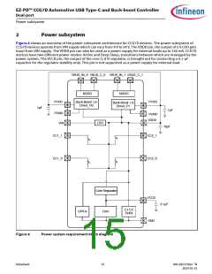
Functional overview
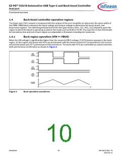
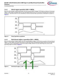
1.4.2
Boost region operation (VIN << VBUS)
When the VIN voltage is significantly lower than the required VBUS voltage, CCG7D devices operate in the boost
region. In this region, the buck side FETs are inactivated, with the sync FET turned off and the buck control FET
turned on. The boost side FETs are controlled as a boost converter with synchronous rectification as shown in
Figure 4.
ON
HG1
(Buck
Control)
OFF
ON
LG1
(Buck
Sync)
OFF
ON
LG2
(Boost
Control)
OFF
ON
HG2
(Boost
Sync)
OFF
Inductor
Current
0
t
Figure 4
Boost operation waveforms
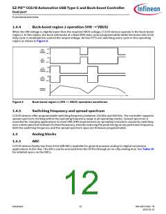
1.4.3
Buck-boost region 1 operation (VIN ~> VBUS)
When the VIN voltage is slightly higher than the required VBUS voltage, CCG7D devices operate in the buck-boost
region 1. In this region, the boost side works at a fixed 20% duty cycle (programmable) while the buck side (LG1
/ HG1) duty cycle is modulated to control the output voltage. All four FETs are switching every cycle in this
operating region as shown in Figure 5.
ON
HG1
(Buck
Control)
OFF
ON
LG1
(Buck
Sync)
OFF
ON
LG2
(Boost
Control)
OFF
ON
HG2
(Boost
Sync)
OFF
Inductor
Current
0
t
Figure 5
Buck-boost region 1 (VIN ~> VBUS) operation waveforms
Datasheet
11
002-28172 Rev. *N
2023-01-31

 INFINEON [ Infineon ]