EZ-PD™ CCG7D Automotive USB Type-C and Buck-boost Controller
Dual-port
Functional overview
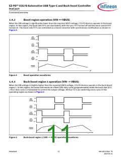
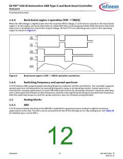
1.4.4
Buck-boost region 2 operation (VIN ~< VBUS)
When the VIN voltage is slightly lower than the required VBUS voltage, CCG7D devices operate in the buck-boost
region 2. In this region, the buck side works at a fixed 80% duty cycle (programmable) while the boost side (LG2)
duty cycle is modulated to control the output voltage. All four FETs are switching every cycle in this operating
region as shown in Figure 6.
ON
HG1
(Buck
Control)
OFF
ON
LG1
(Buck
Sync)
OFF
ON
LG2
(Boost
Control)
OFF
ON
HG2
(Boost
Sync)
OFF
Inductor
Current
0
t
Figure 6
Buck-boost region 2 (VIN ~< VBUS) operation waveforms
1.4.5
Switching frequency and spread spectrum
CCG7D devices offer programmable switching frequency between 150 kHz and 600 kHz. The controller supports
spread spectrum clocking within the operating frequency range in all operating modes. Spread spectrum is
essential for charging applications to meet EMC/EMI requirements by spreading emissions caused by switching
over a wide spectrum instead of a fixed frequency, thereby reducing the peak energy at any particular frequency.
Both the switching frequency and the spread spectrum span are firmware programmable.
1.5
Analog blocks
ADC
1.5.1
CCG7D devices family has three 8-bit SAR ADCs available for general purpose analog-to-digital conversion
applications in the chip. The ADCs can be accessed from the GPIOs through an on-chip analog mux. See Table 29
for detailed specs on the ADCs.
Datasheet
12
002-28172 Rev. *N
2023-01-31

 INFINEON [ Infineon ]