EZ-PD™ CCG7D Automotive USB Type-C and Buck-boost Controller
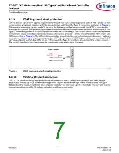
Dual-port
Functional overview
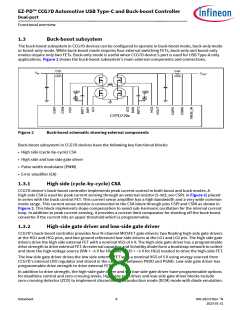
The gate drivers for the switching FETs function at their nominal drive voltage levels (5 V) provided the VIN voltage
is between 5.5 V and 24 V.
1.3.3
Error amplifier (EA)
CCG7D’s buck-boost controller contains two error amplifiers for output voltage and current regulation. The error
amplifier is a trans-conductance type amplifier with single compensation pin (COMP) to ground for both the
voltage and current loops. In voltage regulation, the output voltage is compared with the internal reference
voltage and the output of EA is fed to the PWM block. In current regulation, the average current is sensed by VBUS
high side current sense amplifier through the external resistor. The output of the VBUS CSA is compared with an
internal reference in error amplifier block and EA output is fed to the PWM block. CCG7D’s firmware configures
and controls the integrated programmable error amplifier circuit for achieving the required VBUS voltage output
from the power section.
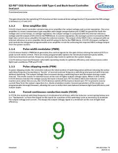
1.3.4
Pulse width modulator (PWM)
CCG7D device family’s PWM block generates the control signals for the gate drivers driving the external FETs in
peak current mode control. There are many programmable options for minimum/maximum pulse width,
minimum/maximum period, frequency and pulse skip levels to optimize the system design.
CCG7D devices have two firmware-selectable operating modes to optimize efficiency and reduce losses under
light load conditions: PSM and FCCM.
1.3.5
Pulse-skipping mode (PSM)
In pulse-skipping mode, the controller reduces the total number of switching pulses without reducing the active
switching frequency by working in “bursts” of normal nominal-frequency switching interspersed with intervals
without switching. The output voltage thus increases during a switching burst and decreases during a quiet
interval. This mode results in minimal losses at the cost of higher output voltage ripple. When in this mode,
CCG7D devices monitor the voltage across the buck or boost sync FET to detect when the inductor current
reaches zero; when this occurs, the CCG7D devices switch off the buck or boost sync FET to prevent reverse
current flow from the output capacitors (i.e. diode emulation mode). Several parameters of this mode are
programmable through firmware, allowing the user to strike their own balance between light load efficiency and
output ripple.
1.3.6
Forced-continuous-conduction mode (FCCM)
In FCCM, the nominal switching frequency is maintained at all times, with the inductor current going below zero
(i.e. “backwards” or from the output to the input) for a portion of the switching cycle as necessary to maintain
the output voltage and current. This keeps the output voltage ripple to a minimum at the cost of light-load
efficiency.
Datasheet
9
002-28172 Rev. *N
2023-01-31

 INFINEON [ Infineon ]