EZ-PD™ CCG7D Automotive USB Type-C and Buck-boost Controller
Dual-port
Functional overview
1.3
Buck-boost subsystem
The buck-boost subsystem in CCG7D devices can be configured to operate in buck-boost mode, buck-only mode
or boost-only mode. While buck-boost mode requires four external switching FETs, buck-only and boost-only
modes require only two FETs. Buck-only mode is useful when CCG7D device’s port is used for USB Type-A only
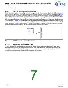
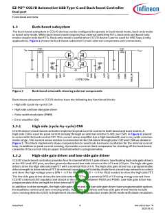
applications. Figure 2 shows the buck-boost subsystem’s main external components and connections.
5 m
5 m
VIN
VOUT
CSR1
CSR2
VDDD
VDDD
CYPD729x
Figure 2
Buck-boost schematic showing external components
Buck-boost subsystem in CCG7D devices have the following key functional blocks:
• High side (cycle-by-cycle) CSA
• High side and low side gate driver
• Pulse width modulator (PWM)
• Error amplifier (EA)
1.3.1
High side (cycle-by-cycle) CSA
CCG7D device’s buck-boost controller implements peak current control in both boost and buck modes. A
high-side CSA is used for peak current sensing through an external resistor (5 mΩ; see CSR1 in Figure 2) placed
in series with the buck control FET. This current sense amplifier has a high bandwidth and a very wide common
mode range. This current sense resistor is connected to the CSA block through pins CSPI and CSNI as shown in
Figure 2. This block implements slope compensation to avoid sub-harmonic oscillation for the internal current
loop. In addition to peak current sensing, it provides a current limit comparator for shutting off the buck-boost
converter if the current hits an upper threshold which is programmable.
1.3.2
High-side gate driver and low-side gate driver
CCG7D’s buck-boost controller provides four N-channel MOSFET gate drivers: two floating high-side gate drivers
at the HG1 and HG2 pins, and two ground referenced low-side drivers at the LG1 and LG2 pin. The high side gate
drivers drive the high side external FET with a nominal VGS of 5 V. The high-side gate driver has a programmable
drive strength to drive external FET. An external capacitor and Schottky diode form a bootstrap network to collect
and store the high voltage source (VIN + ~5 V for HG1 and VBUS + ~5 V for HG2) needed to drive the high-side FET.
The low side gate driver drives the low side external FET with a nominal VGS of 5 V using energy sourced from
CCG7D’s internal LDO regulator and stored in the capacitor between PVDD and PGND. Low-side gate driver has
programmable drive strength to drive external FET.
In addition to drive strength, the high-side gate driver and the low-side gate driver have programmable options
for deadtime control and zero-crossing levels. High-side gate driver and low-side gate driver blocks include
zero-crossing detector (ZCD) to implement discontinuous-conduction mode (DCM) mode with diode emulation.
Datasheet
8
002-28172 Rev. *N
2023-01-31

 INFINEON [ Infineon ]