™
PROFET + 24V
BTT6200-4ESA
Power stage
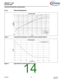
5.3.2
Maximum load inductance
During demagnetization of inductive loads, energy has to be dissipated in the BTT6200-4ESA. This energy can
be calculated with following equation:
V
− V
R
R ⋅ I
− V
L
R
L
S
DS AZ
L
L
L
E = VDS AZ
⋅
⋅
⋅ ln 1 −
+ IL
DS AZ
V
S
Equation 1
The following equation simplifies under the assumption of RL = 0 Ω.
VS
1
E = ⋅ L ⋅ I2 ⋅ 1 −
2
VS − VDS AZ
Equation 2
The energy, which is converted into heat, is limited by the thermal design of the component. See Figure 13 for
the maximum allowed energy dissipation as a function of the load current.
Figure 13
Maximum energy dissipation single pulse, TJ_START = 150°C; VS = 28 V
5.4
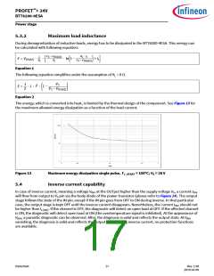
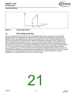
Inverse current capability
In case of inverse current, meaning a voltage VINV at the OUTput higher than the supply voltage VS, a current IINV
will flow from output to VS pin via the body diode of the power transistor (please refer to Figure 14). The output
stage follows the state of the IN pin, except if the IN pin goes from OFF to ON during inverse. In that particular
case, the output stage is kept OFF until the inverse current disappears. Nevertheless, the current IINV should not
be higher than IL(INV). If the channel is OFF, the diagnostic will detect an open load at OFF. If the affected channel
is ON, the diagnostic will detect open load at ON (the overtemperature signal is inhibited). At the appearance of
VINV, a parasitic diagnostic can be observed. Aꢀer, the diagnosis is valid and reflects the output state. At VINV
vanishing, the diagnosis is valid and reflects the output state. During inverse current, no protection functions
are available.
Datasheet
17
Rev. 1.00
2019-03-09

 INFINEON [ Infineon ]