欢迎访问ic37.com |
会员登录 免费注册
发布采购

BTT6200-4ESA 参数 Datasheet PDF下载

BTT6200-4ESA图片预览
型号: BTT6200-4ESA
PDF下载: 下载PDF文件 查看货源
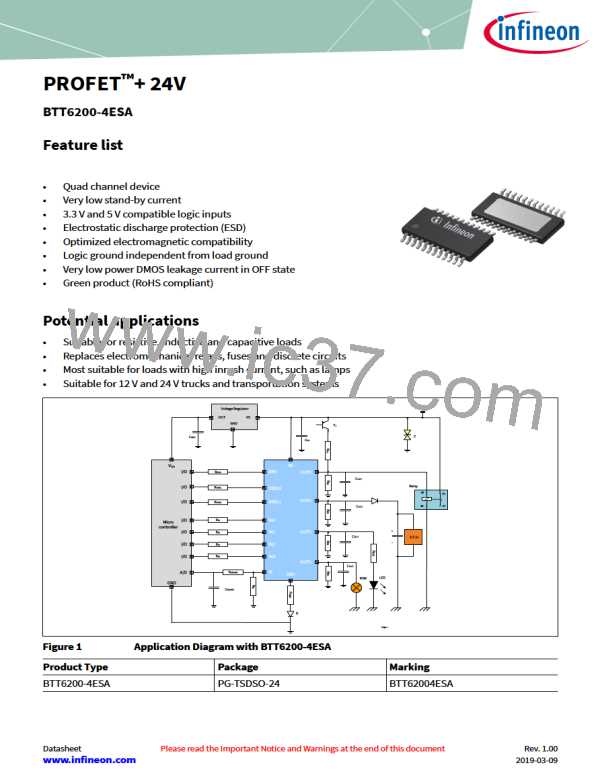
内容描述: [The power transistor is built by an N-channel vertical power MOSFET with charge pump. The device is integrated in Smart6 HV technology. It is specially designed to drive lamps up to R10 W 24 V or R5 W 12 V, as well as LEDs in the harsh automotive environment.]
分类和应用:
文件页数/大小: 51 页 / 1248 K
品牌: INFINEON [ Infineon ]
 浏览型号BTT6200-4ESA的Datasheet PDF文件第12页浏览型号BTT6200-4ESA的Datasheet PDF文件第13页浏览型号BTT6200-4ESA的Datasheet PDF文件第14页浏览型号BTT6200-4ESA的Datasheet PDF文件第15页浏览型号BTT6200-4ESA的Datasheet PDF文件第17页浏览型号BTT6200-4ESA的Datasheet PDF文件第18页浏览型号BTT6200-4ESA的Datasheet PDF文件第19页浏览型号BTT6200-4ESA的Datasheet PDF文件第20页  
PROFET + 24V  
BTT6200-4ESA  
Power stage  
5.3  
Inductive load  
5.3.1  
Output clamping  
When switching OFF inductive loads with high side switches, the voltage VOUT drops below ground potential,  
because the inductance intends to continue driving the current. To prevent the destruction of the device by  
avalanche due to high voltages, there is a voltage clamp mechanism ZDS(AZ) implemented that limits negative  
output voltage to a certain level (VS - VDS(AZ)). Please refer to Figure 11 and Figure 12 for details. Nevertheless,  
the maximum allowed load inductance is limited.  
VS  
ZDS(AZ)  
VDS  
INx  
LOGIC  
IL  
VBAT  
GND  
ZGND  
OUTx  
VOUT  
VIN  
L, RL  
Output_clamp.vsd  
Figure 11  
Output clamp  
IN  
t
VOUT  
VS  
t
VS-VDS(AZ)  
IL  
t
Switching an inductance.vsd  
Figure 12  
Switching an inductive load timing  
Datasheet  
16  
Rev. 1.00  
2019-03-09  
 复制成功!