™
PROFET + 24V
BTT6200-4ESA
Power stage
5
Power stage
The power stages are built using an N-channel vertical power MOSFET (DMOS) with charge pump.
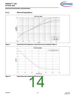
5.1
Output ON-state resistance
The ON-state resistance RDS(ON) depends on the supply voltage as well as the junction temperature TJ. Figure 9
shows the dependencies in terms of temperature and supply voltage for the typical ON-state resistance. The
behavior in reverse polarity is described in Chapter 6.4.
Figure 9
Typical ON-state resistance
A high signal at the input pin (see Chapter 8) causes the power DMOS to switch ON with a dedicated slope,
which is optimized in terms of EMC emission.
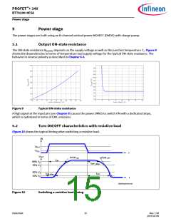
5.2
Turn ON/OFF characteristics with resistive load
Figure 10 shows the typical timing when switching a resistive load.
IN
VIN_H
VIN_L
t
VOUT
dV/dt ON
dV/dt OFF
tON
90% VS
tOFF_delay
70% VS
30% VS
tON_delay
tOFF
10% VS
t
Switching times.vsd
Figure 10
Switching a resistive load timing
Datasheet
15
Rev. 1.00
2019-03-09

 INFINEON [ Infineon ]