®
PROFET BTS 740 S2
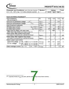
Parameter and Conditions, each of the two channels
Symbol
Values
Unit
at Tj = -40...+150°C, V = 12 V unless otherwise specified
bb
min
typ
max
7.0
Input and Status Feedback20)
Input resistance
(see circuit page 9)
RI
3.0
4.5
kΩ
Input turn-on threshold voltage
Input turn-off threshold voltage
Input threshold hysteresis
VIN(T+)
VIN(T-)
--
1.5
--
--
--
3.5
--
V
V
∆ VIN(T)
0.5
--
--
V
Off state input current
On state input current
VIN = 0.4 V: IIN(off)
VIN = 5 V: IIN(on)
1
50
90
--
µA
µA
µs
20
--
50
400
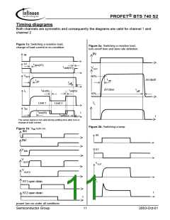
Delay time for status with open load
after Input neg. slope (see diagram page 13)
td(ST OL3)
Status delay after positive input slope
(not subject to production test, specified by design)
tdon(ST)
tdoff(ST)
--
--
13
1
--
--
µs
µs
V
Status delay after negative input slope
(not subject to production test, specified by design)
Status output (open drain)
Zener limit voltage T =-40...+150°C, IST = +1.6 mA: VST(high)
5.4
6.1
6.9
j
--
--
--
--
0.4
0.7
ST low voltage
T =-40...+25°C, IST = +1.6 mA: VST(low)
j
T = +150°C, IST = +1.6 mA:
j
Status leakage current, V = 5 V,
T =25 ... +150°C: IST(high)
j
--
--
2
µA
ST
20)
If ground resistors R
are used, add the voltage drop across these resistors.
GND
Semiconductor Group
7
2003-Oct-01

 INFINEON [ Infineon ]