®
PROFET BTS 740 S2
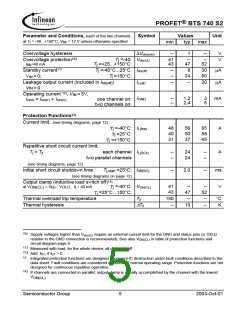
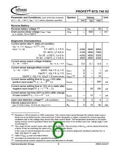
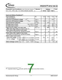
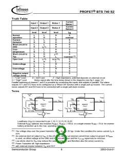
Electrical Characteristics
Parameter and Conditions, each of the two channels
Symbol
Values
Unit
at Tj = -40...+150°C, V = 12 V unless otherwise specified
bb
min
--
typ
max
Load Switching Capabilities and Characteristics
On-state resistance (V to OUT); I = 5 A
L
bb
each channel,
mΩ
Tj = 25°C: RON
Tj = 150°C:
27
54
30
60
two parallel channels, Tj = 25°C:
14
50
15
Output voltage drop limitation at small load
currents, see page 14
VON(NL)
--
--
--
mV
A
I = 0.5 A
L
T =-40...+150°C:
j
Nominal load current
one channel active: IL(NOM)
two parallel channels active:
4.9
7.8
5.5
8.5
6)
Device on PCB , T = 85°C, T ≤ 150°C
a
j
Output current while GND disconnected or pulled up7);
IL(GNDhigh)
--
--
8
mA
V
= 30 V, V = 0, see diagram page 10
IN
bb
Turn-on time8)
Turn-off time
IN
IN
to 90% VOUT
to 10% VOUT: toff
:
ton
25
25
70
80
150
200
µs
RL = 12 Ω
Slew rate on8)
10 to 30% VOUT, RL = 12 Ω:
Slew rate off8)
70 to 40% VOUT, RL = 12 Ω:
dV/dton
0.1
0.1
--
--
1 V/µs
1 V/µs
-dV/dtoff
Operating Parameters
)
Operating voltage9
Vbb(on)
5.0
3.2
--
--
--
34
V
V
V
Undervoltage shutdown
Undervoltage restart
Vbb(under)
5.0
T =-40...+25°C: Vbb(u rst)
4.5
5.5
6.0
j
T =+150°C:
j
Undervoltage restart of charge pump
see diagram page 13
T =-40...+25°C: Vbb(ucp)
--
--
4.7
--
6.5
7.0
V
V
j
T =150°C:
j
Undervoltage hysteresis
∆Vbb(under)
--
0.5
--
∆V
bb(under)
= V
bb(u rst)
- V
bb(under)
Overvoltage shutdown
Overvoltage restart
Vbb(over)
Vbb(o rst)
34
33
--
--
43
--
V
V
Device on 50mm*50mm*1.5mm epoxy PCB FR4 with 6cm2 (one layer, 70µm thick) copper area for V
connection. PCB is vertical without blown air. See page 15
not subject to production test, specified by design
6
)
bb
7
)
)
8
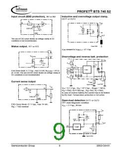
See timing diagram on page 11.
9)
At supply voltage increase up to V = 4.7 V typ without charge pump, V
≈V - 2 V
bb
bb
OUT
Semiconductor Group
4
2003-Oct-01

 INFINEON [ Infineon ]