®
PROFET BTS 740 S2
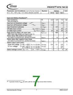
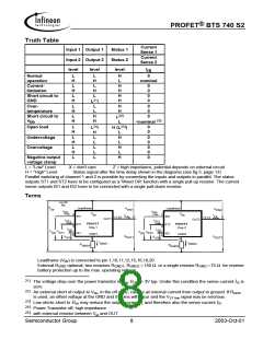
Truth Table
Current
Sense 1
Current
Sense 2
Input 1 Output 1
Input 2 Output 2
Status 1
Status 2
level
level
level
I
IS
Normal
L
H
L
H
L
L
H
L
H
L
H
L
H
H
H
H
0
operation
Current-
limitation
Short circuit to
GND
nominal
0
0
0
0
21
H
)
L
Over-
temperature
Short circuit to
L
H
L
L
L
H
H
H
H
0
0
0
22)
L
23)
V
bb
H
L
<nominal
24
25)
Open load
L
H
0
0
)
L
H (L
L
)
H
L
L
L
L
L
Undervoltage
Overvoltage
L
H
L
H
L
H
L
H
L
0
0
0
0
0
Negative output
voltage clamp
L = "Low" Level
H = "High" Level
H
X = don't care
Z = high impedance, potential depends on external circuit
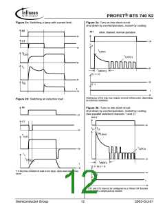
Status signal after the time delay shown in the diagrams (see fig 5. page 13)
Parallel switching of channel 1 and 2 is possible by connecting the inputs and outputs in parallel. The status
outputs ST1 and ST2 have to be configured as a 'Wired OR' function with a single pull-up resistor. The current
sense outputs IS1 and IS2 have to be connected with a single pull-down resistor.
Terms
I
bb
V
Leadframe
Leadframe
V
V
bb
ON1
ON2
I
I
IN1
IN2
I
V
V
3
4
bb
7
8
I
bb
I
L1
IN1
L2
IN2
17,18
13,14
OUT1
OUT2
I
ST1
I
ST2
PROFET
Chip 1
PROFET
Chip 2
ST1
ST2
I
IS1
IS2
V
V
V
V
ST2
IN2
ST1
IN1
IS1
R
IS2
GND1
2
GND2
6
5
9
V
V
V
OUT2
V
OUT1
IS1
IS2
I
I
GND1
GND2
R
GND1
GND2
Leadframe (V ) is connected to pin 1,10,11,12,15,16,19,20
bb
External R
optional; two resistors R , R
GND1
=150 Ω or a single resistor R
=75 Ω for reverse
GND
GND2
GND
battery protection up to the max. operating voltage.
21)
22)
The voltage drop over the power transistor is Vbb-VOUT > 3V typ. Under this condition the sense current IIS is
zero
An external short of output to Vbb, in the off state, causes an internal current from output to ground. If RGND
is used, an offset voltage at the GND and ST pins will occur and the VST low signal may be errorious.
23)
24)
25)
Low ohmic short to Vbb may reduce the output current IL and therefore also the sense current IIS.
Power Transistor off, high impedance
with external resistor between VBB and OUT
Semiconductor Group
8
2003-Oct-01

 INFINEON [ Infineon ]