®
PROFET BTS 740 S2
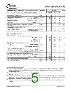
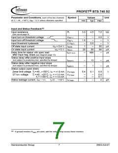
Parameter and Conditions, each of the two channels
Symbol
Values
Unit
at Tj = -40...+150°C, V = 12 V unless otherwise specified
bb
min
--
typ
max
--
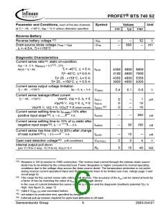
Overvoltage hysteresis
∆Vbb(over)
1
V
V
Overvoltage protection10)
T =-40: Vbb(AZ)
41
43
--
--
j
I
=40 mA
T =+25...+150°C:
47
52
bb
j
)
Standby current11
VIN = 0;
Tj =-40°C...25°C: Ibb(off)
--
--
8
24
30
50
µA
µA
T =150°C:
j
Leakage output current (included in Ibb(off)
VIN = 0
)
IL(off)
--
--
20
Operating current 12), VIN = 5V,
IGND
--
--
1.2
2.4
3
6
mA
IGND = IGND1 + IGND2
,
one channel on:
two channels on:
Protection Functions13)
Current limit, (see timing diagrams, page 12)
Tj =-40°C: IL(lim)
Tj =25°C:
Tj =+150°C:
48
40
31
56
50
37
65
58
45
A
A
Repetitive short circuit current limit,
Tj = Tjt
each channel IL(SCr)
two parallel channels
--
--
24
24
--
--
(see timing diagrams, page 12)
Initial short circuit shutdown time
Tj,start =25°C: toff(SC)
--
2.0
--
ms
V
(see timing diagrams on page 12)
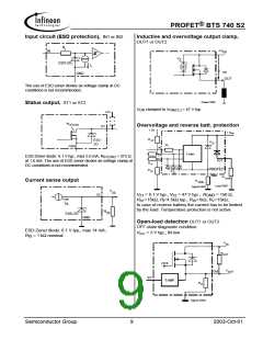
Output clamp (inductive load switch off)14)
at V
ON(CL)
= V - V
bb OUT
, I = 40 mA
Tj =-40°C: VON(CL)
Tj =25°C...150°C:
41
43
--
47
--
--
52
--
L
Thermal overload trip temperature
Thermal hysteresis
Tjt
150
--
°C
K
∆Tjt
10
--
10)
Supply voltages higher than Vbb(AZ) require an external current limit for the GND and status pins (a 150 Ω
resistor in the GND connection is recommended). See also V
in table of protection functions and
ON(CL)
circuit diagram page 9.
Measured with load; for the whole device; all channels off
11)
12)
13
Add I , if I > 0
ST
ST
Integrated protection functions are designed to prevent IC destruction under fault conditions described in the
data sheet. Fault conditions are considered as "outside" normal operating range. Protection functions are not
designed for continuous repetitive operation.
14)
If channels are connected in parallel, output clamp is usually accomplished by the channel with the lowest
V
ON(CL)
Semiconductor Group
5
2003-Oct-01

 INFINEON [ Infineon ]