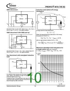
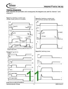
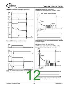
®
PROFET BTS 740 S2
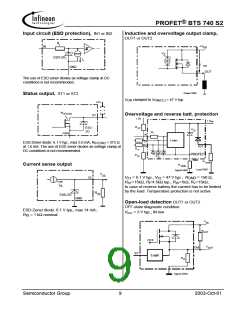
Input circuit (ESD protection), IN1 or IN2
Inductive and overvoltage output clamp,
OUT1 or OUT2
R
I
+V
bb
IN
V
Z
ESD-ZDI
I
I
V
ON
GND
OUT
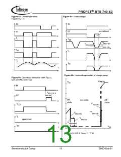
The use of ESD zener diodes as voltage clamp at DC
conditions is not recommended.
Power GND
Status output, ST1 or ST2
V
ON
clamped to V = 47 V typ.
ON(CL)
+5V
R
ST(ON)
Overvoltage and reverse batt. protection
ST
+ 5V
+ V
bb
R
ESD-
ZD
ST
V
Z2
R
GND
I
IN
Logic
ST
IS
ESD-Zener diode: 6.1 V typ., max 5.0 mA; R
ST(ON)
at 1.6 mA. The use of ESD zener diodes as voltage clamp at
DC conditions is not recommended.
< 375 Ω
OUT
R
R
V
PRO FET
IS
V
Z1
GND
R
Load
Current sense output
R
GND
Signal GND
Load GND
V
IS
IS
V
Z1
= 6.1 V typ., V = 47 V typ., R
= 150 Ω,
Z2
GND
R
=15kΩ, R =4.5kΩ typ., R =1kΩ, R =15kΩ,
ST
I
IS
V
I
IS
In case of reverse battery the current has to be limited
by the load. Temperature protection is not active
R
IS
ESD-ZD
GND
Open-load detection OUT1 or OUT2
OFF-state diagnostic condition:
ESD-Zener diode: 6.1 V typ., max 14 mA;
= 1 kΩ nominal
VOUT > 3 V typ.; IN low
R
IS
V
bb
R
EXT
OFF
V
Out
OUT
ST
Logic
R
O
Signal GND
Semiconductor Group
9
2003-Oct-01

 INFINEON [ Infineon ]