BTS 712 N1
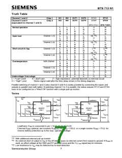
Truth Table
IN1
IN3
IN2
IN4
OUT1
OUT3
OUT2
OUT4
ST1/2
ST3/4
ST1/2
ST3/4
Channel 1 and 2
Channel 3 and 4
Chip 1
Chip 2
(equivalent to channel 1 and 2)
BTS 711L1 BTS 712N1
Normal operation
Open load
L
L
H
H
L
L
H
L
H
X
L
L
H
L
H
X
L
X
H
L
H
X
X
X
L
H
L
H
L
H
X
L
L
H
L
H
X
L
L
H
L
H
X
X
X
L
H
X
L
L
H
H
Z
Z
H
L
H
X
H
H
H
L
H
X
L
L
L
L
L
X
X
L
L
H
L
H
L
H
X
Z
Z
H
L
H
X
H
H
H
L
L
L
X
X
L
L
L
H
H
H
H
H
H
H
H
L
H
H
L
13)
Channel 1 (3)
Channel 2 (4)
Channel 1 (3)
Channel 2 (4)
both channel
H(L
)
)
H
L
13)
H(L
H
L
14)
H
H
14)
Short circuit to V
L
L
bb
H
H
H
15)
14)
H(L
)
14)
L
L
H
H
H
H
L
L
H
L
H
L
H
15)
H(L
)
Overtemperature
H
L
L
H
L
H
L
Channel 1 (3)
Channel 2 (4)
Undervoltage/ Overvoltage
H
L = "Low" Level
H = "High" Level
X = don't care
Z = high impedance, potential depends on external circuit
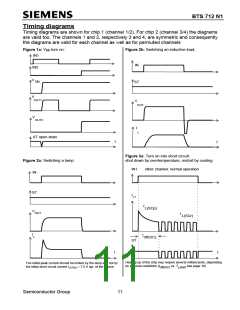
Status signal valid after the time delay shown in the timing diagrams
Parallel switching of channel 1 and 2 (also channel 3 and 4) is easily possible by connecting the inputs and
outputs in parallel (see truth table). If switching channel 1 to 4 in parallel, the status outputs ST1/2 and ST3/4
have to be configured as a 'Wired OR' function with a single pull-up resistor.
Terms
I
bb
V
V
V
ON1
ON3
Leadframe
Leadframe
bb
V
V
ON2
ON4
I
I
I
I
IN1
IN2
IN3
IN4
V
V
bb
bb
3
5
7
9
I
I
I
I
IN1
IN3
L1
L3
18
17
14
13
OUT1
OUT2
OUT3
OUT4
PROFET
Chip 1
PROFET
Chip 2
IN2
IN4
L2
L4
I
I
ST3/4
ST1/2
4
8
ST1/2
ST3/4
V
V
V
V
GND1/2
2
GND3/4
6
V
V
IN4
IN1
IN3
IN2
ST1/2
V
ST3/4
V
OUT1
OUT3
V
V
OUT4
I
I
OUT2
GND1/2
GND3/4
R
R
GND1/2
GND3/4
Leadframe (V ) is connected to pin 1,10,11,12,15,16,19,20
bb
External R
optional; two resistors R
,R
GND3/4
=150 Ω or a single resistor R
=75 Ω for
GND
GND1/2
GND
reverse battery protection up to the max. operating voltage.
13)
14)
With additional external pull up resistor
An external short of output to Vbb in the off state causes an internal current from output to ground. If RGND is
used, an offset voltage at the GND and ST pins will occur and the VST low signal may be errorious.
15)
Low resistance to V may be detected by no-load-detection
bb
Semiconductor Group
7

 INFINEON [ Infineon ]