BTS 712 N1
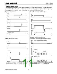
Timing diagrams
Timing diagrams are shown for chip 1 (channel 1/2). For chip 2 (channel 3/4) the diagrams
are valid too. The channels 1 and 2, respectively 3 and 4, are symmetric and consequently
the diagrams are valid for each channel as well as for permuted channels
Figure 1a: V turn on:
Figure 2b: Switching an inductive load,
bb
IN1
IN2
IN
V
bb
ST
V
OUT1
V
OUT
V
OUT2
I
L
ST open drain
t
t
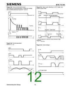
Figure 3a: Turn on into short circuit:
Figure 2a: Switching a lamp:
shut down by overtemperature, restart by cooling
IN1
other channel: normal operation
IN
ST
IL1
I
L(SCp)
VOUT
I
L(SCr)
IL
t
off(SC)
ST
t
t
Heating up of the chip may require several milliseconds, depending
on external conditions (t vs. T see page 10)
The initial peak current should be limited by the lamp and not by
the initial short circuit current IL(SCp) = 7.5 A typ. of the device.
off(SC)
j,start
Semiconductor Group
11

 INFINEON [ Infineon ]