BTS 712 N1
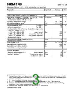
Maximum Ratings at Tj = 25°C unless otherwise specified
Parameter
Symbol
Values
Unit
Load current (Short-circuit current, see page 5)
IL
self-limited
60
A
V
4)
Load dump protection2) VLoadDump = UA + Vs, UA = 13.5 V VLoad dump
RI3) = 2 Ω, td = 200 ms; IN= low or high,
each channel loaded with RL = 7.1Ω,
Operating temperature range
Storage temperature range
Power dissipation (DC)5
(all channels active)
Tj
Tstg
-40 ...+150
-55 ...+150
°C
W
Ta = 25°C: Ptot
Ta = 85°C:
3.6
1.9
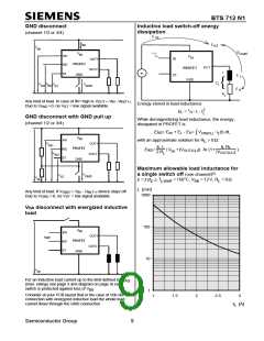
Inductive load switch-off energy dissipation, single pulse
Vbb =12V, Tj,start =150°C5),
150
320
800
mJ
IL = 1.9 A, ZL = 66mH, 0Ω
IL = 2.8 A, ZL = 66mH, 0Ω
IL = 4.4 A, ZL = 66mH, 0Ω
see diagrams on page 9
one channel: EAS
two parallel channels:
four parallel channels:
Electrostatic discharge capability (ESD)
(Human Body Model)
VESD
1.0
kV
Input voltage (DC)
VIN
IIN
IST
-10 ... +16
±2.0
V
mA
Current through input pin (DC)
Current through status pin (DC)
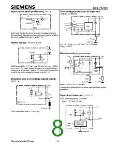
see internal circuit diagram page 8
±5.0
Thermal resistance
junction - soldering point5),6)
each channel: Rthjs
16 K/W
junction - ambient5)
one channel active: Rthja
all channels active:
44
35
2)
Supply voltages higher than Vbb(AZ) require an external current limit for the GND and status pins, e.g. with a
150 Ω resistor in the GND connection and a 15 kΩ resistor in series with the status pin. A resistor for input
protection is integrated.
3)
4)
5)
R = internal resistance of the load dump test pulse generator
I
VLoad dump is setup without the DUT connected to the generator per ISO 7637-1 and DIN 40839
Device on 50mm*50mm*1.5mm epoxy PCB FR4 with 6cm2 (one layer, 70µm thick) copper area for V
connection. PCB is vertical without blown air. See page 14
bb
6)
Soldering point: upper side of solder edge of device pin 15. See page 14
Semiconductor Group
3

 INFINEON [ Infineon ]