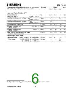
BTS 712 N1
Parameter and Conditions, each of the four channels Symbol
Values
Unit
at Tj = 25 °C, V = 12 V unless otherwise specified
bb
min
typ
max
Input and Status Feedback12)
Input resistance
RI
2.5
1.7
1.5
3.5
--
6
3.5
--
kΩ
V
(see circuit page 8)
Tj =-40..+150°C:
Input turn-on threshold voltage
VIN(T+)
VIN(T-)
∆ VIN(T)
Tj =-40..+150°C:
Tj =-40..+150°C:
Input turn-off threshold voltage
Input threshold hysteresis
--
V
--
1
0.5
--
--
V
Off state input current
Tj =-40..+150°C:
VIN = 0.4 V: IIN(off)
VIN = 5 V: IIN(on)
td(ST OL3)
50
µA
On state input current
Tj =-40..+150°C:
20
--
50
90
--
µA
µs
Delay time for status with open load
(see timing diagrams, page 12)
220
Status output (open drain)
Zener limit voltage Tj =-40...+150°C, IST = +1.6 mA: VST(high)
5.4
--
--
6.1
--
--
--
0.4
0.6
V
ST low voltage
Tj =-40...+25°C, IST = +1.6 mA: VST(low)
Tj = +150°C, IST = +1.6 mA:
12)
If ground resistors R
are used, add the voltage drop across these resistors.
GND
Semiconductor Group
6

 INFINEON [ Infineon ]