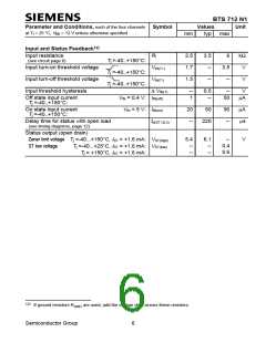
BTS 712 N1
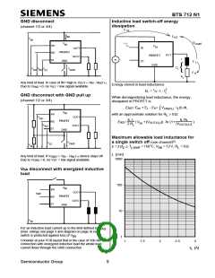
GND disconnect
Inductive load switch-off energy
dissipation
(channel 1/2 or 3/4)
E
bb
I
E
bb
AS
V
bb
E
E
V
Load
bb
IN1
IN2
ST
V
bb
IN
OUT1
OUT2
PROFET
O U T
PROFET
L
=
GND
V
ST
L
G N D
Z
V
V
V
L
IN1 IN2
GND
{
ST
E
R
R
L
Any kind of load. In case of IN=high is V
OUT
Due to VGND > 0, no V = low signal available.
ST
≈ V -V
.
IN IN(T+)
Energy stored in load inductance:
2
L
1
E = / ·L·I
L
2
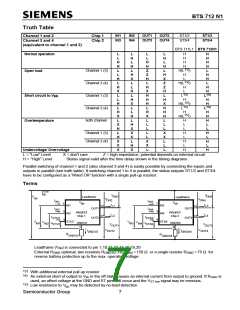
GND disconnect with GND pull up
(channel 1/2 or 3/4)
While demagnetizing load inductance, the energy
dissipated in PROFET is
E
= Ebb + EL - ER= VON(CL)·i (t) dt,
L
AS
∫
V
bb
IN1
with an approximate solution for R > 0Ω:
L
OUT1
OUT2
V
IN1
I ·L
L
I ·R
L
L
OUT(CL)
PROFET
IN2
ST
E
AS
=
(V +|V
|) ln (1+
OUT(CL)
)
bb
2·R
|V
|
V
L
IN2
GND
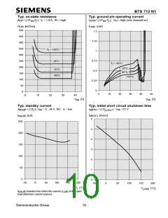
Maximum allowable load inductance for
5)
V
a single switch off (one channel)
V
GND
ST
V
bb
L = f (I ); T
= 150°C, V = 12 V, R = 0 Ω
L
j,start
bb
L
L [mH]
1000
Any kind of load. If V
> V - V
IN
device stays off
GND
IN(T+)
Due to V
> 0, no V = low signal available.
ST
GND
V
disconnect with energized inductive
bb
load
100
10
V
bb
IN1
OUT1
high
PROFET
IN2
ST
OUT2
GND
V
bb
For an inductive load current up to the limit defined by E
(max. ratings see page 3 and diagram on page 9) each
AS
switch is protected against loss of V
.
bb
1
1
Consider at your PCB layout that in the case of Vbb dis-
connection with energized inductive load the whole load
current flows through the GND connection.
1.5
2
2.5
3
I
[A]
L
Semiconductor Group
9

 INFINEON [ Infineon ]