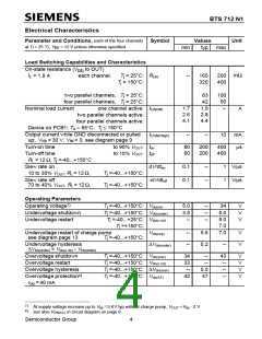
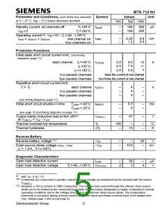
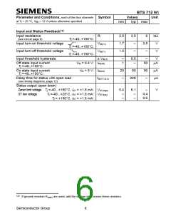
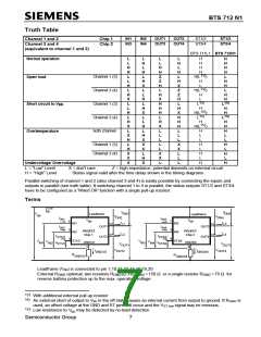
BTS 712 N1
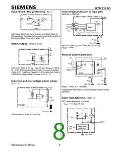
Input circuit (ESD protection), IN1...4
Overvoltage protection of logic part
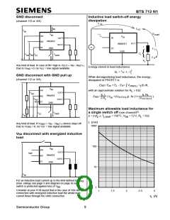
GND1/2 or GND3/4
R
+ V
bb
I
IN
V
Z2
R
I
IN
IN
ESD-ZDI
I
I
Logic
GND
ST
RST
V
Z1
ESD zener diodes are not to be used as voltage clamp at
DC conditions. Operation in this mode may result in a drift of
the zener voltage (increase of up to 1 V).
GND
RGND
Signal GND
Status output, ST1/2 or ST3/4
V
Z1
= 6.1 V typ., V = 47 V typ., R = 3.5 kΩ typ.,
Z2
I
R
GND
= 150 Ω
+5V
R
ST(ON)
ST
Reverse battery protection
V
-
+ 5V
bb
ESD-
ZD
RST
GND
RI
IN
ESD-Zener diode: 6.1 V typ., max 5.0 mA; R
ST(ON)
< 380 Ω
OUT
ST
at 1.6 mA, ESD zener diodes are not to be used as voltage
clamp at DC conditions. Operation in this mode may result in
a drift of the zener voltage (increase of up to 1 V).
Power
Inverse
Diode
Logic
GND
RGND
RL
Inductive and overvoltage output clamp,
OUT1...4
Power GND
Signal GND
R
GND
= 150 Ω, R = 3.5 kΩ typ,
I
+V
bb
Temperature protection is not active during inverse current
operation.
V
Z
VON
OUT
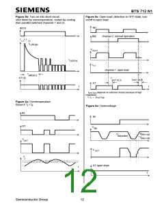
Open-load detection, OUT1...4
OFF-state diagnostic condition:
V
OUT
> 3 V typ.; IN low
PROFET
Power GND
V
ON
clamped to V = 47 V typ.
ON(CL)
OFF
I
V
L(OL)
OUT
Open load
detection
Logic
unit
Signal GND
Semiconductor Group
8

 INFINEON [ Infineon ]