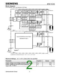
BTS 712 N1
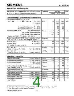
Parameter and Conditions, each of the four channels Symbol
at Tj = 25 °C, V = 12 V unless otherwise specified
bb
Values
typ max
Unit
min
Standby current, all channels off
VIN = 0
Tj =25°C: Ibb(off)
Tj =150°C:
--
--
180
160
300
300
µA
Operating current 9), VIN = 5V, Tj =-40...+150°C
IGND
-- 0.35
0.8 mA
2.8
IGND = IGND1/2 + IGND3/4
,
one channel on:
four channels on:
--
1.2
Protection Functions
Initial peak short circuit current limit, (see timing
diagrams, page 11)
each channel, Tj =-40°C: IL(SCp)
Tj =25°C:
5.5
4.5
2.5
9.5
7.5
4.5
13
11
7
A
A
Tj =+150°C:
two parallel channels
four parallel channels
Repetitive short circuit current limit,
twice the current of one channel
four times the current of one channel
Tj = Tjt
each channel IL(SCr)
two parallel channels
four parallel channels
--
--
--
4
4
4
--
--
--
(see timing diagrams, page 11)
Initial short circuit shutdown time
Tj,start =-40°C: toff(SC)
Tj,start = 25°C:
--
--
5.5
4
-- ms
--
(see page 10 and timing diagrams on page 11)
Output clamp (inductive load switch off)10)
at VON(CL) = Vbb - VOUT
VON(CL)
--
47
--
V
Thermal overload trip temperature
Thermal hysteresis
Tjt
150
--
--
--
--
°C
K
∆Tjt
10
Reverse Battery
Reverse battery voltage 11)
-Vbb
--
--
--
32
V
Drain-source diode voltage (V > V
)
-VON
610
-- mV
out
bb
IL =-1.9A, Tj =+150°C
Diagnostic Characteristics
Open load detection current
Open load detection voltage
IL(off)
--
2
30
3
--
4
µA
Tj =-40..+150°C: VOUT(OL)
V
9)
10)
Add I , if I > 0
ST
ST
If channels are connected in parallel, output clamp is usually accomplished by the channel with the lowest
V
ON(CL)
11)
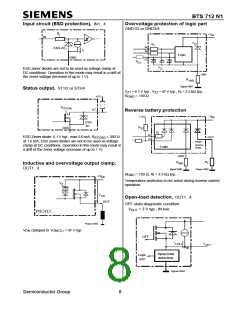
Requires a 150 Ω resistor in GND connection. The reverse load current through the intrinsic drain-source
diode has to be limited by the connected load. Note that the power dissipation is higher compared to normal
operating conditions due to the voltage drop across the intrinsic drain-source diode. The temperature
protection is not active during reverse current operation! Input and Status currents have to be limited (see
max. ratings page 3 and circuit page 8).
Semiconductor Group
5

 INFINEON [ Infineon ]