Target Data Sheet BTS555
Parameter and Conditions
Symbol
Values
Unit
at Tj = -40 ... +150°C, V = 12V unless otherwise specified
bb
min
typ
max
Input
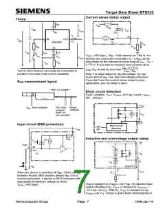
Input and operating current (see diagram page 13) IIN(on)
--
--
1
2
mA
IN grounded (V =0)
IN
Input current for turn-off19)
IIN(off)
--
80
µA
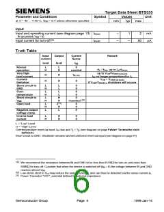
Truth Table
Input
current
Output
level
Current
Sense
Remark
level
I
IS
Normal
L
H
L
H
0
=IL / kilis, up to IIS=IIS,lim
operation
Very high
load current
Current-
limitation
Short circuit to
GND
Over-
temperature
Short circuit to
nominal
up to VON=VON(Fold back)
IIS no longer proportional to IL
VON > VON(Fold back)
H
H
H
H
IIS, lim
0
if VON>VON(SC), shutdown will occure
L
H
L
H
L
H
L
H
L
L
L
L
L
H
H
Z21
H
L
0
0
0
0
0
V
bb
<nominal 20)
)
Open load
0
0
0
Negative output
voltage clamp
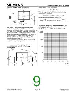
Inverse load
current
L
H
H
H
0
0
L = "Low" Level
H = "High" Level
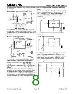
Overtemperature reset via input: IIN=low and T < T (see diagram on page Fehler! Textmarke nicht
j
jt
definiert.)
Short circuit to GND: Shutdown remains latched until next reset via input (see diagram on page14)
19)
We recommend the resistance between IN and GND to be less than 0.5kΩ for turn-on and more than
500kΩ for turn-off. Consider that when the device is switched off (I =0) the voltage between IN and GND
IN
reaches almost V
.
bb
20)
21)
Low ohmic short to Vbb may reduce the output current IL and can thus be detected via the sense current IIS.
Power Transistor "OFF", potential defined by external impedance.
Semiconductor Group
Page 6
1998-Jan-14

 INFINEON [ Infineon ]