Target Data Sheet BTS555
Energy stored in load inductance:
E = 1/ ·L·I2
Inverse load current operation
L
2
L
While demagnetizing load inductance, the energy
dissipated in PROFET is
V
bb
V
bb
- I
L
E
= Ebb + EL - ER= VON(CL)·iL(t) dt,
AS
OUT
IN
V
∫
+
-
PROFET
with an approximate solution for R > 0Ω:
L
IS
V
+
-
OUT
I ·L
I ·RL
|VOUT(CL)|
L
L
E
AS
=
(Vbb + |VOUT(CL)|) ln (1+
)
I
2·RL
IS
V
IN
R
IS
IS
Maximum allowable load inductance for
a single switch off
The device is specified for inverse load current
operation (VOUT > Vbb > 0V). The current sense
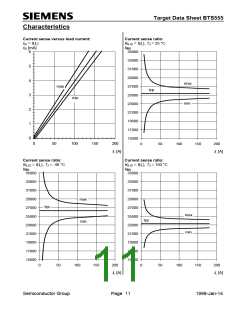
L = f (I ); T
= 150°C, V = 12V, R = 0Ω
L
j,start
bb
L
feature is not available during this kind of operation (IIS
= 0). With IIN = 0 (e.g. input open) only the intrinsic
drain source diode is conducting resulting in consi-
derably increased power dissipation. If the device is
switched on (VIN = 0), this power dissipation is
decreased to the much lower value RON(INV) * I2
(specifications see page 4).
L [mH]
10000
1000
100
10
Note: Temperature protection during inverse load
current operation is not possible!
Inductive load switch-off energy
dissipation
E
bb
E
AS
E
Load
V
bb
i (t)
L
V
bb
OUT
IN
PROFET
E
L
1
0
L
IS
2.5
5
7.5
10
12.5
15
[A]
{
Z
L
I
E
R
R
IN
R
L
I
IS
L
Semiconductor Group
Page 9
1998-Jan-14

 INFINEON [ Infineon ]