Target Data Sheet BTS555
Parameter and Conditions
Symbol
Values
Unit
at Tj = -40 ... +150°C, V = 12V unless otherwise specified
bb
min
typ
max
Operating Parameters
Operating voltage (VIN =0) Fehler! Textmarke nicht definiert., Vbb(on)
5.0
--
--
34
V
V
12)
13)
Undervoltage shutdown
VbIN(u)
3.5
4.5
Undervoltage start of charge pump
see diagram page 15
VbIN(ucp)
--
60
62
--
5
--
66
15
25
6.5
--
--
V
Overvoltage protection14)
Tj =-40°C: VbIN(Z)
V
Ibb =15mA
Tj =25...+150°C:
Standby current
IIN =0
Tj =-40...+25°C: Ibb(off)
Tj =150°C:
25
60
µA
--
Protection Functions
Short circuit current limit (Tab to pins 1,5)
VON =12V, time until shutdown max. 300µs Tc =-40°C: IL(SCp)
Tc =25°C:
--
tbd
tbd
460
400
280
--
tbd
tbd
A
Tc =+150°C:
Short circuit shutdown delay after input current
positive slope, VON > VON(SC)
td(SC)
80
--
300
µs
min. value valid only if input "off-signal" time exceeds 30µs
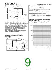
Output clamp 15)
(inductive load switch off)
IL= 40 mA: -VOUT(CL)
IL= 20 A:
--
--
15
17
--
--
V
Output clamp (inductive load switch off)
at VOUT = Vbb - VON(CL) (e.g. overvoltage)
IL= 40 mA
VON(CL)
39
--
42
6
46
--
V
V
Short circuit shutdown detection voltage
(pin 3 to pins 1,5)
VON(SC)
12)
13)
For all voltages 0 ... 34 V the device is fully protected against overtemperature and short circuit.
VbIN = Vbb - VIN see diagram on page 8. When VbIN increases from less than VbIN(u) up to VbIN(ucp) = 5V
(typ.) the charge pump is not active and VOUT ≈Vbb -3V.
See also VON(CL) in circuit diagram on page 9.
This output clamp can be "switched off" by using an additional diode at the IS-Pin (see page8). If the diode
is used, VOUT is clamped to Vbb- VON(CL) at inductive load switch off.
14)
15)
Semiconductor Group
Page 4
1998-Jan-14

 INFINEON [ Infineon ]