Target Data Sheet BTS555
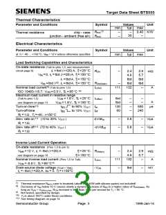
Thermal Characteristics
Parameter and Conditions
Symbol
Values
Unit
min
--
typ
max
7)
RthJC
chip - case:
K/W
-- 0.40
30
Thermal resistance
--
junction - ambient (free air): RthJA
--
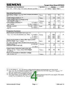
Electrical Characteristics
Parameter and Conditions
Symbol
Values
Unit
at Tj = -40 ... +150°C, V = 12V unless otherwise specified
bb
min
typ
max
Load Switching Capabilities and Characteristics
On-state resistance (Tab to pins 1,5, see measurement
circuit page 8)
IL =tbd (>=20) A, T =25°C:
j
RON
--
2.4
4.6
tbd
tbd
132
2.9
5.7
tbd
tbd
--
mΩ
VIN =0, IL =tbd (>=20) A, T =150°C:
j
IL =tbd A, T =150°C:
j
Vbb =tbd V8), IL =tbd A, T =150°C: RON(Static)
--
j
Nominal load current9) (Tab to pins 1,5)
IL(ISO)
111
A
ISO 10483-1/6.7: VON =0.5V, T =85°C 10)
c
Maximum load current in resistive range
(Tab to pins 1,5)
VON =1.8V, T =25°C: IL(Max)
tbd
tbd
130
60
--
--
--
--
--
--
c
A
see diagram on page 13
Turn-on time11)
VON =1.8V, T =150°C:
c
I
I
to 90% VOUT: ton
to 10% VOUT: toff
550
240
µs
IN
IN
Turn-off time
RL =1Ω , Tj =-40...+150°C
Slew rate on11) (10 to 30% VOUT
RL =1Ω
Slew rate off11) (70 to 40% VOUT
RL =1Ω
)
dV/dton
--
--
0.8
0.8
-- V/µs
-- V/µs
)
-dV/dtoff
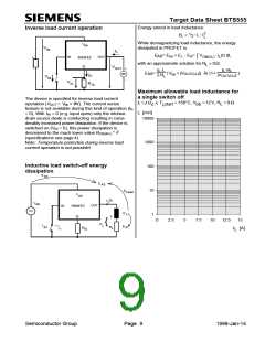
Inverse Load Current Operation
On-state resistance (Pins 1,5 to pin 3)
VbIN =12 V, IL =- tbd (>=20) A
see diagram on page 10
T =25°C:
T =150°C:
j
--
111
--
2.4
4.6
2.9
5.7
--
RON(inv)
mΩ
j
Nominal inverse load current (Pins 1,5 to Tab)
IL(inv)
132
A
VON =-0.5V, T =85°C10
c
Drain-source diode voltage (V > V
)
bb
-VON
tbd
-- mV
out
I
-
I = 0,
L = tbd (>=20)A, Tj =+150°C
IN
7)
Thermal resistance RthCH case to heatsink (about 0.25 K/W with silicone paste) not included!
8)
Decrease of Vbb below 10 V causes slowly a dynamic increase of RON to a higher value of RON(Static). As
long as VbIN > VbIN(u) max, RON increase is less than 10 % per second for TJ < 85 °C.
Not tested, specified by design.
TJ is about 105°C under these conditions.
See timing diagram on page 14.
9)
10)
11)
Semiconductor Group
Page 3
1998-Jan-14

 INFINEON [ Infineon ]