Target Data Sheet BTS555
the inductive load, but higher peak power dissipation in
the PROFET.
V
load
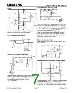
disconnect with energized inductive
bb
Provide a current path with load current capability by
using a diode, a Z-diode, or a varistor. (VZL <72 V or
VZb <30 V if RIN=0). For higher clamp voltages
currents at IN and IS have to be limited to 250 mA.
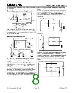
Overvoltage protection of logic part
+ V
bb
R
V
V
bb
Z,IN
Z,IS
Version a:
R
IN
IN
Logic
V
V
bb
V
OUT
bb
PROFET
IS
IS
OUT
IN
PROFET
V
R
Z,VIS
R
V
IS
Signal GND
R
=120Ω typ., VZ,IN = VZ,IS = 66V typ., RIS =1kΩ
bb
V
ZL
nominal. Note that when overvoltage exceeds 71V typ.
a voltage above 5V can occur between IS and GND, if
RV, VZ,VIS are not used.
Version b:
Reverse battery protection
V
-
V
bb
bb
V
bb
Rbb
OUT
IN
PROFET
IN
IS
OUT
Power
RIN
Logic
Transistor
V
Zb
IS
DS
RL
Note that there is no reverse battery protection when
using a diode without additional Z-diode V , VZb.
ZL
RV
RIS
D
Version c: Sometimes a neccessary voltage clamp is
given by non inductive loads RL connected to the
same switch and eliminates the need of clamping
circuit:
Signal GND
Power GND
RV ≥1kΩ, RIS =1kΩ nominal. Add RIN for reverse
battery protection in applications with V above
bb
1
1
1
16V16); recommended value:
0.1A
+
+
=
RIN RIS RV
0.1A
RIN |Vbb| - 12V
1
V
V
bb
bb
if DS is not used (or
=
if DS
R
L
|Vbb| - 12V
is used).
OUT
IN
PROFET
To minimize power dissipation at reverse battery
operation, the summarized current into the IN and IS
pin should be about 120mA. The current can be
provided by using a small signal diode D in parallel to
the input switch, by using a MOSFET input switch or
by proper adjusting the current through RIS and RV.
IS
Semiconductor Group
Page 8
1998-Jan-14

 INFINEON [ Infineon ]