High Current PN Half Bridge
BTN8982TA
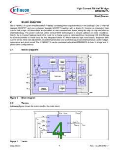
General Product Characteristics
4.3
Thermal Resistance
Pos.
4.3.1
Parameter
Symbol
Limit Values
Unit
Conditions
Min.
Typ.
Max.
1)
Thermal Resistance
Junction-Case, High Side Switch
RthJC(HS)
–
0.55
0.8
1.6
–
K/W
R
thjc(HS) = ΔTj(HS)/ Pv(HS)
1)
4.3.2
4.3.3
Thermal Resistance
Junction-Case, Low Side Switch
RthJC(LS)
–
–
1.1
19
K/W
K/W
R
thjc(LS) = ΔTj(LS)/ Pv(LS)
1) 2)
Thermal Resistance
Junction-Ambient
RthJA
1) Not subject to production test, specified by design
2) Specified RthJA value is according to Jedec JESD51-2,-5,-7 at natural convection on FR4 2s2p board; The Product
(Chip+Package) was simulated on a 76.2 x 114.3 x 1.5 mm board with 2 inner copper layers (2 x 70µm Cu, 2 x 35µm Cu).
Where applicable a thermal via array under the exposed pad contacted the first inner copper layer.
Data Sheet
8
Rev. 1.0, 2013-05-17

 INFINEON [ Infineon ]