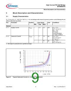
High Current PN Half Bridge
BTN8982TA
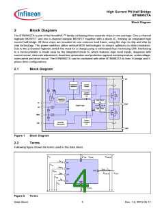
Block Diagram
2
Block Diagram
The BTN8982TA is part of the NovalithIC™ family containing three separate chips in one package: One p-channel
highside MOSFET and one n-channel lowside MOSFET together with a driver IC, forming an integrated high
current half-bridge. All three chips are mounted on one common lead frame, using the chip on chip and chip by
chip technology. The power switches utilize vertical MOS technologies to ensure optimum on state resistance.
Due to the p-channel highside switch the need for a charge pump is eliminated thus minimizing EMI. Interfacing
to a microcontroller is made easy by the integrated driver IC which features logic level inputs, diagnosis with
current sense, slew rate adjustment, dead time generation and protection against overtemperature, undervoltage,
overcurrent and short circuit. The BTN8982TA can be combined with other BTN8982TA to form H-bridge and 3-
phase drive configurations.
2.1
Block Diagram
VS
Undervolt.
detection
Current
Sense
Current
Limitation
HS
Overtemp.
detection
Gate Driver
HS
IS
IN
OUT
Digital Logic
LS off
HS off
Gate Driver
LS
INH
SR
Current
Limitation
LS
Slewrate
Adjustment
GND
Figure 1
Block Diagram
2.2
Terms
Following figure shows the terms used in this data sheet.
VS
IVS , -ID(HS)
VDS(HS)
I
IN
VS
IN
VIN
IINH
INH
SR
IOUT , IL
VDS(LS)
OUT
VINH
ISR
VOUT
VSR
IIS
IS
GND
VIS
IGND, ID(LS)
Figure 2
Terms
Data Sheet
4
Rev. 1.0, 2013-05-17

 INFINEON [ Infineon ]