High Current PN Half Bridge
BTN8982TA
General Product Characteristics
4
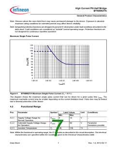
General Product Characteristics
4.1
Absolute Maximum Ratings
Absolute Maximum Ratings 1)
Tj = -40 °C to +150 °C; all voltages with respect to ground, positive current flowing into pin
(unless otherwise specified)
Pos.
Parameter
Symbol
Limit Values
Max.
Unit
Conditions
Min.
Voltages
4.1.1
Supply Voltage
VS
-0.3
40
–
V
V
V
V
V
V
–
4.1.2
Drain-Source Voltage High Side
VDS(HS) -40
Tj ≥ 25°C
Tj < 25°C
Tj ≥ 25°C
Tj < 25°C
–
-38
–
4.1.3
4.1.4
Drain-Source Voltage Low Side
Logic Input Voltage
VDS(LS)
–
40
38
5.3
–
VIN
-0.3
VINH
4.1.5
Voltage at SR Pin
VSR
-0.3
1.0
40
40
V
V
V
–
–
–
4.1.6
Voltage between VS and IS Pin
Voltage at IS Pin
VS -VIS -0.3
4.1.7
VIS
-20
Currents
4.1.8
HS/LS Continuous Drain Current2) ID(HS)
-50
-44
50
44
A
A
A
TC < 85°C
switch active
ID(LS)
TC < 125°C
switch active
4.1.9
HS/LS Pulsed Drain Current2)
ID(HS)
ID(LS)
tpulse = 10ms
single pulse
-117
-104
117
104
TC < 85°C
TC < 125°C
4.1.10 HS/LS PWM Current2)
ID(HS)
ID(LS)
A
A
f = 1kHz, DC = 50%
TC < 85°C
TC < 125°C
-68
-60
68
60
f = 20kHz, DC = 50%
TC < 85°C
TC < 125°C
-70
-62
70
62
Temperatures
4.1.11 Junction Temperature
4.1.12 Storage Temperature
ESD Susceptibility
Tj
-40
-55
150
150
°C
°C
–
–
Tstg
4.1.13 ESD Resistivity HBM
IN, INH, SR, IS
VESD
kV
HBM3)
-2
-6
2
6
OUT, GND, VS
1) Not subject to production test, specified by design
2) Maximum reachable current may be smaller depending on current limitation level
3) ESD susceptibility, HBM according to ANSI/ESDA/JEDEC JS-001 (1,5kΩ, 100pF)
Data Sheet
6
Rev. 1.0, 2013-05-17

 INFINEON [ Infineon ]