High Current PN Half Bridge
BTN8982TA
Block Description and Characteristics
5.2
Power Stages
The power stages of the BTN8982TA consist of a p-channel vertical DMOS transistor for the high side switch and
a n-channel vertical DMOS transistor for the low side switch. All protection and diagnostic functions are located in
a separate top chip. Both switches allow active freewheeling and thus minimizing power dissipation during PWM
control.
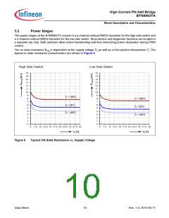
The on state resistance RON is dependent on the supply voltage VS as well as on the junction temperature Tj. The
typical on state resistance characteristics are shown in Figure 6.
High Side Switch
Low Side Switch
Tj = 150°C
Tj = 150°C
Tj = 25°C
Tj = -40°C
Tj = 25°C
Tj = -40°C
VS [V]
VS [V]
Figure 6
Typical ON State Resistance vs. Supply Voltage
Data Sheet
10
Rev. 1.0, 2013-05-17

 INFINEON [ Infineon ]