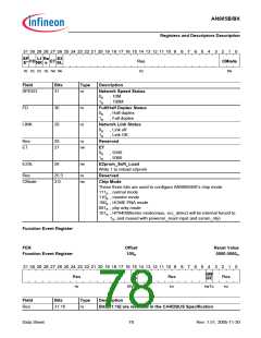
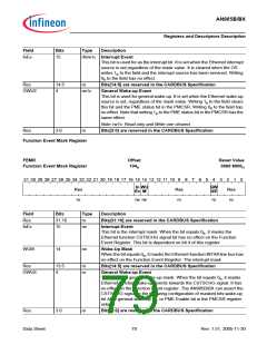
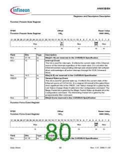
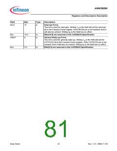
AN985B/BX
Registers and Descriptors Description
8.3
PHY Registers
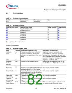
Table 14
Module
PHY
Registers Address Space
Base Address
End Address
0000 0006H
Note
0000 0000H
Table 15
Registers Overview
Register Short Name
Register Long Name
Register 0(MII Control)
Register 1(Status)
Register 2
Register 3
Register 4
Offset Address Page Number
R0
R1
R2
R3
R4
R5
R6
0H
1H
2H
3H
4H
5H
6H
83
85
87
87
88
89
90
Register 5
Register 6
The register is addressed wordwise.
Standard abbreviations:
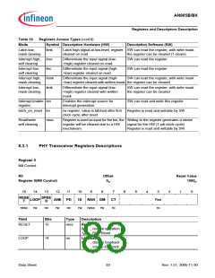
Table 16
Mode
Registers Access Types
Symbol Description Hardware (HW)
Description Software (SW)
read/write
rw
Register is used as input for the HW
Register is read and writable by SW
read
r
Register is written by HW (register
Value written by software is ignored by
between input and output -> one cycle hardware; that is, software may write any
delay)
value to this field without affecting hardware
behavior (= Target for development.)
write
w
Register is writable by SW
read/write
hardware
affected
rwh
Register can be modified by HW
Register can be modified by HW, but the
priority SW versus HW has to be specified
rwv
ro
Read only
Register is set by HW (register between SW can only read this register
input and output -> one cycle delay)
Read virtual
rv
Physically, there is no new register, the SW can only read this register
input of the signal is connected directly
to the address multiplexer.
Latch high,
self clearing
Latch low,
self clearing
lhsc
llsc
Latch high signal at high level, clear on SW can read the register
read
Latch high signal at low-level, clear on SW can read the register
read
Latch high,
mask clearing
lhmk
Latch high signal at high level, register SW can read the register, with write mask
cleared with written mask
the register can be cleared (1 clears)
Data Sheet
82
Rev. 1.51, 2005-11-30

 INFINEON [ Infineon ]