AN985B/BX
Registers and Descriptors Description
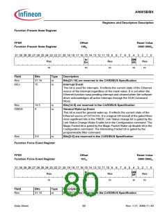
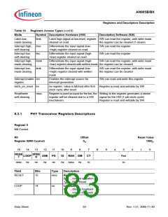
Table 16
Mode
Registers Access Types (cont’d)
Symbol Description Hardware (HW)
Description Software (SW)
Latch low,
llmk
ihsc
ilsc
Latch high signal at low-level, register SW can read the register, with write mask
mask clearing
cleared on read
the register can be cleared (1 clears)
SW can read the register
Interrupt high,
self clearing
Interrupt low,
self clearing
Differentiate the input signal (low-
>high) register cleared on read
Differentiate the input signal (high-
>low) register cleared on read
SW can read the register
Interrupt high,
mask clearing
Interrupt low,
mask clearing
ihmk
ilmk
Differentiate the input signal (high-
SW can read the register, with write mask
>low) register cleared with written mask the register can be cleared
Differentiate the input signal (low-
>high) register cleared with written
mask
SW can read the register, with write mask
the register can be cleared
Interrupt enable ien
register
latch_on_reset lor
Enables the interrupt source for
interrupt generation
rw register, value is latched after first
clock cycle after reset
SW can read and write this register
Register is read and writable by SW
Read/write
self clearing
rwsc
Register is used as input for the hw, the Writing to the register generates a strobe
register will be cleared due to a HW
mechanism.
signal for the HW (1 pdi clock cycle)
Register is read and writable by SW.
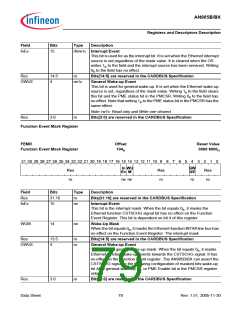
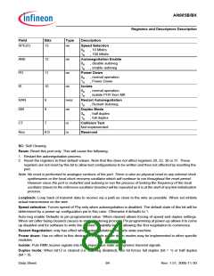
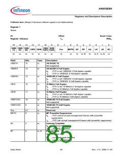
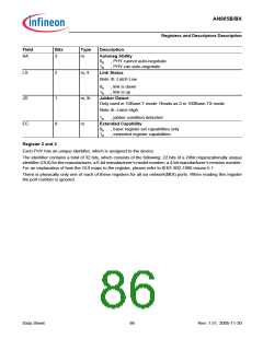
8.3.1
PHY Transceiver Registers Descriptions
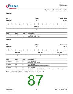
Register 0
MII Control
R0
Offset
0H
Reset Value
Register 0(MII Control)
1000H
ꢀꢁ
ꢀꢂ
/223
UZ
ꢀꢃ
ꢀꢄ
ꢀꢀ
ꢀꢅ
,6
UZ
ꢆ
ꢇ
ꢈ
ꢉ
ꢁ
ꢂ
ꢃ
5HV
UR
ꢄ
ꢀ
ꢅ
5(6(
7
63((
'
$1( 3'
5$1 '0
UZVF UZ
&7
UR
UZVF
UZ
UZ
UZ
Field
RESET
Bits
15
Type
rwsc
Description
Reset
0B
1B
, normal operation
, PHY Reset
LOOP
14
rw
Loopback
0B
1B
, disable loopback
, enable loopback
Data Sheet
83
Rev. 1.51, 2005-11-30

 INFINEON [ Infineon ]