AN985B/BX
Registers and Descriptors Description
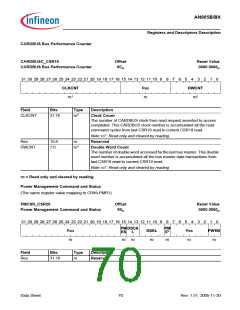
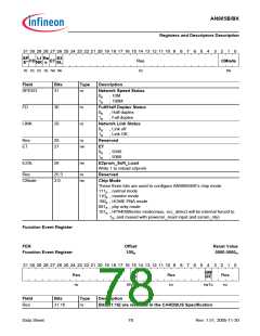
Field
ADDR
DATA
Bits
25:8
7:0
Type
rw
rw
Description
Flash ROM Address
Read/Write Data of Flash ROM
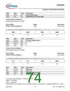
Physical Address Register 0
Automatically recall from EEPROM
PAR0_CSR25
Physical Address Register 0
Offset
A4H
Reset Value
xxxx xxxxH
ꢀꢁ ꢀꢂ ꢃꢄ ꢃꢅ ꢃꢆ ꢃꢇ ꢃꢈ ꢃꢉ ꢃꢀ ꢃꢃ ꢃꢁ ꢃꢂ ꢁꢄ ꢁꢅ ꢁꢆ ꢁꢇ ꢁꢈ ꢁꢉ ꢁꢀ ꢁꢃ ꢁꢁ ꢁꢂ ꢄ
ꢅ
ꢆ
ꢇ
ꢈ
ꢉ ꢀ ꢃ ꢁ ꢂ
3$%ꢀ
3$%ꢁ
3$%ꢂ
3$%ꢃ
UZ
UZ
UZ
UZ
Field
PAB3
PAB2
PAB1
PAB0
Bits
Type
rw
rw
rw
rw
Description
Physical Address Byte n
n = 0 to 3
31:24
23:16
15:8
7:0
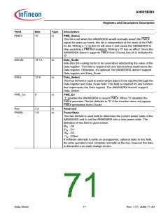
Physical Address Register 1
Automatically recall from EEPROM
PAR1_CSR26
Physical Address Register 1
Offset
A8H
Reset Value
xxxx xxxxH
ꢀꢁ ꢀꢂ ꢃꢄ ꢃꢅ ꢃꢆ ꢃꢇ ꢃꢈ ꢃꢉ ꢃꢀ ꢃꢃ ꢃꢁ ꢃꢂ ꢁꢄ ꢁꢅ ꢁꢆ ꢁꢇ ꢁꢈ ꢁꢉ ꢁꢀ ꢁꢃ ꢁꢁ ꢁꢂ ꢄ
ꢅ
ꢆ
ꢇ
ꢈ
ꢉ ꢀ ꢃ ꢁ ꢂ
5HV
UR
5HV
UR
3$%ꢀ
3$%ꢁ
UZ
UZ
Field
Res
Res
PAB5
PAB4
Bits
31:24
23:16
15:8
7:0
Type
ro
ro
rw
rw
Description
Reserved
Reserved
Physical Address Byte 5
Physical Address Byte 4
For example, physical address = 00-00-e8-11-22-33
PAR0 = 11 e8 00 00
PAR1 = xx xx 33 22
PAR0 and PAR1 are readable, but can be written only if the receive state is in stopped (CSR5 bit19-17 = 000).
Data Sheet 74 Rev. 1.51, 2005-11-30

 INFINEON [ Infineon ]