AN985B/BX
Registers and Descriptors Description
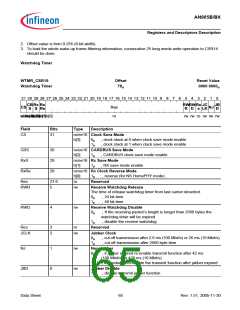
Field
Bits
Type
Description
AUXCL
30:28
ro
Aux Current
Should be 0.
PMEPS
PMEPE
PCI
27
26
25
24
rw
rw
rw
rw
PMEP Select
0B
1B
, positive pulse
, negative pulse
PMEP Pin Enable
0B
1B
, disable(for old board)
, enable
PCI Pad
0B
1B
, apply CARDBUS Pad in CARDBUS Mode. No effect in PCI Mode
, apply PCI Pad in CARDBUS Mode(for twinhead notebook)
PS
PMES Sticky
0B
, pmez auto de-asserted: pmez will be disasserted by power up
after wakeup event trigger.
1B
, pmez sticky: Vcc_detect has no impact to pmez disasserts
4_3L
RFS
23
rw
rw
4_3LED
0B
1B
, 3 LED scheme
, 4 LED scheme
22:21
Receive FIFO Size Control
00B , reserved
01B , reserved
10B , 2K
11B , 1K
CRD
PM
20
19
rw
ro
Clock Run (clk-run pin) Disable
1B
, disables the function of clock run supports to CARDBUS
Power Management
Enables the AN985B/BX whether to activate the Power Management
abilities. When this bit is set into “0” the AN985B/BX will set the Cap_Ptr
register to zero, indicating no CARDBUS compliant power management
capabilities.The value of this bit will be mapped to NC-bit 20 of CR1.In
CARDBUS Power Management mode, the Wake-up events include
“Wake-up Frame Received”, “Magic Packet Received” and “Link Status
Changed” depends on the CSR13 settings.
APM
18
rw
APM Mode
This bit is effective when PM (csr18 [19]) = 1.
LWS
Res
PLS
17
16:9
8
rw
ro
rw
Should be 0
Reserved
PMEP Pulse Length Select
0B
1B
, long pulse 50ms
, short pulse 100us for test purpose
D3A
7
6
rw
rw
D3_cold APM Mode Enable
PMEZ can be asserted without the impact of PME_EN
RWP
Reset Wake-up Pattern Data Register Pointer
0B
1B
, Normal
, Reset
Data Sheet
68
Rev. 1.51, 2005-11-30

 INFINEON [ Infineon ]