AN985B/BX
Registers and Descriptors Description
Power Management Register 0
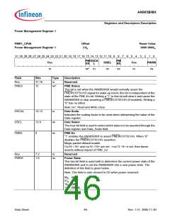
PMR0_CR48
Power Management Register 0
Offset
C0H
Reset Value
FE82 0001H
ꢀꢁ ꢀꢂ ꢃꢄ ꢃꢅ ꢃꢆ ꢃꢇ ꢃꢈ ꢃꢉ ꢃꢀ ꢃꢃ ꢃꢁ ꢃꢂ ꢁꢄ ꢁꢅ ꢁꢆ ꢁꢇ ꢁꢈ ꢁꢉ ꢁꢀ ꢁꢃ ꢁꢁ ꢁꢂ ꢄ
ꢅ ꢆ ꢇ ꢈ ꢉ ꢀ ꢃ ꢁ ꢂ
'ꢀ 'ꢁ
'6 5H 30
30(6
$8;&
9(5
1,3
&$3,'
6
6
,
V (&
UR
UR UR
UR
UR UR UR
UR
UR
UR
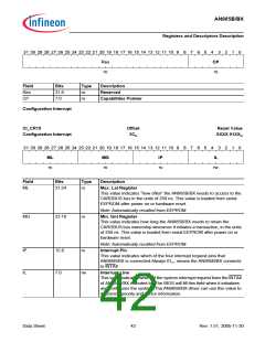
Field
PMES
Bits
31:27
Type
ro
Description
PME Support
The AN985B/BX will assert PME#/CSTSCHG signal while in the D0, D1,
D2, D3 power state. The AN985B/BX supports Wake-up from the above
states.
D2S
26
ro
ro
ro
D2 Support
The AN985B/BX supports D2 Power Management State.
D1S
25
D1 Support
The AN985B/BX supports D1 Power Management State.
AUXC
24:22
Aux Current
These three bits report the maximum 3.3 Vaux current requirements for
AN985B/BX. If bit 31 of PMR0 is ‘1’, the default value is 0101B, means
AN985B/BX need 100 mA to support remote wake-up in D3cold power
state.
DSI
21
ro
Device Specific Initialization
The Device Specific Initialization bit indicates whether special
initialization of this function is required before the generic class device
driver is able to use it.
0B
, indicates that the function does not require a device specific
initialization sequence following transition to the D0 un-initialized
state
Res
PMEC
20
19
ro
ro
Reserved
PME Clock
When “1” indicates that the AN985B/BX relies on the presence of the
CARDBUS clock for PME#/CSTSCHG operation. While “0” indicates the
no CARDBUS clock is required for the AN985B/BX to generate
PME#/CSTSCHG.
VER
NIP
18:16
15:8
ro
ro
Version
The value of 010B indicates that the AN985B/BX complies with Revision
1.0a of the CARDBUS Power Management Interface Specification.
Next Item Pointer
This value is always 0H, indicates that there is no additional items in the
Capabilities List.
Data Sheet
44
Rev. 1.51, 2005-11-30

 INFINEON [ Infineon ]