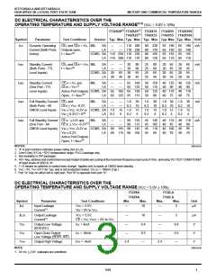
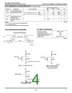
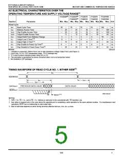
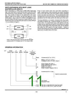
IDT7132SA/LA AND IDT7142SA/LA
HIGH-SPEED 2K x 8 DUAL-PORT STATIC RAM
MILITARY AND COMMERCIAL TEMPERATURE RANGES
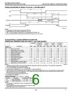
AC ELECTRICAL CHARACTERISTICS OVER THE
OPERATING TEMPERATURE AND SUPPLY VOLTAGE RANGE(7)8M824S258M824S30 7132158M824S4
7132X20(1) 7132X25(8)
7142X25(8)
7132X35
7132X55 7132X100
7142X35
7142X55 7142X100
Symbol
Parameter
Min. Max. Min. Max. Min. Max. Min. Max. Min. Max.
Unit
Busy Timing (For Master lDT7130 Only)
tBAA
tBDA
tBAC
tBDC
tWDD
tWH
BUSY Access Time from Address
BUSY Disable Time from Address
BUSY Access Time from Chip Enable
BUSY Disable Time from Chip Enable
Write Pulse to Data Delay(2)
—
—
—
—
—
12
—
5
20
20
20
20
50
—
35
—
25
—
—
—
40
30
—
—
—
—
—
15
—
5
20
20
20
20
50
—
35
—
35
—
—
—
50
35
—
—
—
—
—
20
—
5
20
20
20
20
60
—
35
—
35
—
—
—
60
35
—
—
—
—
—
20
—
5
30
30
30
30
80
—
55
—
50
—
—
—
80
55
—
—
—
—
—
20
—
5
50
50
ns
ns
ns
ns
ns
ns
ns
ns
ns
50
50
120
—
Write Hold After BUSY(6)
tDDD
tAPS
tBDD
Write Data Valid to Read Data Delay(2)
Arbitration Priority Set-up Time(3)
BUSY Disable to Valid Data(4)
100
—
—
5
—
5
—
5
—
5
—
5
65
Busy Timing (For Slave IDT7140 Only)e
tWB
tWH
Write to BUSY Input(5)
Write Hold After BUSY(6)
Write Pulse to Data Delay(2)
Write Data Valid to Read Data Delay(2)
0
0
0
0
0
—
—
ns
ns
12
—
—
15
—
—
20
—
—
20
—
—
20
—
—
tWDD
tDDD
120
100
ns
ns
NOTES:
2689 tbl 11
1. Com'l Only, 0°C to +70°C temperature range. PLCC package only.
2. Port-to-port delay through RAM cells from the writing port to the reading port, refer to “Timing Waveform of Write with Port -to-Port Read and BUSY."
3. To ensure that the earlier of the two ports wins.
4. tBDD is a calculated parameter and is the greater of 0, tWDD – tWP (actual), or tDDD – tDW (actual).
5. To ensure that a write cycle is inhibited on port 'B' during contention on port 'A'..
6. To ensure that a write cycle is completed on port 'B' after contention on port 'A'.
7. “X” in part numbers indicates power rating (S or L).
8. Not available in DIP package
(1,2,3)
TIMING WAVEFORM OF WRITE WITH PORT-TO-PORT READ AND BUSY
tWC
ADDR’A’
MATCH
t
WP
R/W’A’
t
DW
t
DH
DATAIN’A’
VALID
(1)
tAPS
ADDR’B’
BUSY’B’
MATCH
tBDD
tBDA
tWDD
DATAOUT’B’
VALID
tDDD
NOTES:
2692 drw 11
1. To ensure that the earlier of the two ports wins. tAPS is ignored for Slave (IDT7142).
2. CEL = CER = VIL.
3. OE = VIL for the reading port.
4. All timing is the same for the left and right ports. Port 'A' may be either the left or right
port. Port 'B' is opposite from port 'A'.
6.02
8

 IDT [ INTEGRATED DEVICE TECHNOLOGY ]