IDT7132SA/LA AND IDT7142SA/LA
HIGH-SPEED 2K x 8 DUAL-PORT STATIC RAM
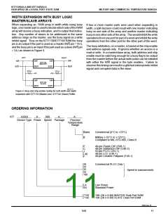
MILITARY AND COMMERCIAL TEMPERATURE RANGES
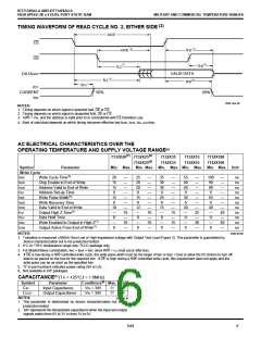
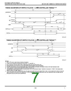
TIMING WAVEFORM OF WRITE CYCLE NO. 1, (R/W CONTROLLED TIMING)(1,5,8)
t
WC
ADDRESS
OE
(7)
t
HZ
t
AW
CE
(7)
(2)
WP
(6)
AS
(3)
t
t
t
WR
tHZ
R/W
(7)
t
OW
t
WZ
(4)
(4)
DATA OUT
DATA IN
t
DW
tDH
2692 drw 09
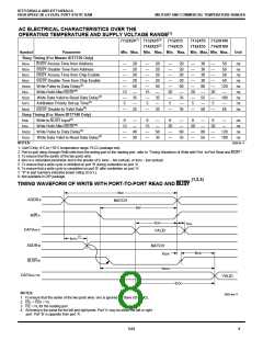
TIMING WAVEFORM OF WRITE CYCLE NO. 2, (CE CONTROLLED TIMING)(1,5)
tWC
ADDRESS
CE
tAW
(6)
AS
(2)
tEW
(3)
t
tWR
R/W
tDW
tDH
DATA IN
2692 drw 10
NOTES:
1. R/W or CE must be High during all address transitions.
2. A write occurs during the overlap (tEW or tWP) of CE = VIL and R/W= VIL.
3. tWR is measured from the earlier of CE or R/W going High to the end of the write cycle.
4. During this period, the l/O pins are in the output state and input signals must not be applied.
5. If the CE Low transition occurs simultaneously with or after the R/W Low transition, the outputs remain in the High-impedance state.
6. Timing depends on which enable signal (CE or R/W) is asserted last.
7. This parameter is determined be device characterization, but is not production tested. Transition is measured +/- 500mV from steady state
with the Output Test Load (Figure 2).
8. If OE is low during a R/W controlled write cycle, the write pulse width must be the larger of tWP or (tWZ + tDW) to allow the I/O drivers to turn off
data to be placed on the bus for the required tDW. If OE is High during a R/W controlled write cycle, this requirement does not apply and the
write pulse can be as short as the specified tWP.
6.02
7

 IDT [ INTEGRATED DEVICE TECHNOLOGY ]