IDT7132SA/LA AND IDT7142SA/LA
HIGH-SPEED 2K x 8 DUAL-PORT STATIC RAM
MILITARY AND COMMERCIAL TEMPERATURE RANGES
FUNCTIONAL DESCRIPTION
TRUTH TABLES
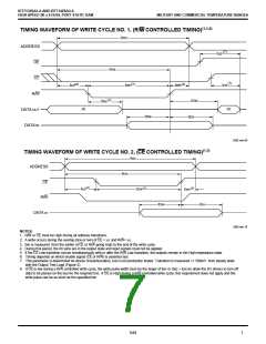
The IDT7132/IDT7142 provides two ports with separate
control,addressandI/Opinsthatpermitindependentaccess
for reads or writes to any location in memory. The IDT7132/
IDT7142 has an automatic power down feature controlled by
CE. The CE controls on-chip power down circuitry that
permits the respective port to go into a standby mode when
notselected(CE=VIL). Whenaportisenabled, accesstothe
entire memory array is permitted.
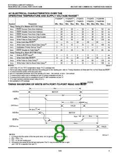
TABLE I — NON-CONTENTION
READ/WRITE CONTROL(4)
Left or Right Port(1)
R/W CE OE
D0–7
Function
X
H
X
Z
Port Disabled and in Power-
Down Mode, ISB2 or ISB4
X
H
X
Z
CER = CEL = VIH, Power-Down
Mode, ISB1 or ISB3
L
L
L
L
X
L
DATAIN Data Written Into Memory(2)
DATAOUT Data in Memory Output on Port(3)
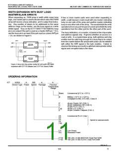
BUSY LOGIC
H
H
Busy Logic provides a hardware indication that both ports of
the RAM have accessed the same location at the same time.
It also allows one of the two accesses to proceed and signals
the other side that the RAM is “Busy”. The busy pin can then
be used to stall the access until the operation on the other
side is completed. If a write operation has been attempted
from the side that receives a busy indication, the write signal
is gated internally to prevent the write from proceeding.
H
Z
High Impedance Outputs
NOTES:
1. A0L – A10L ≠ A0R – A10R.
2. If BUSY = L, data is not written.
3. If BUSY = L, data may not be valid, see tWDD and tDDD timing.
4. 'H' = VIH, 'L' = VIL, 'X' = DON’T CARE, 'Z' = High-impedance.
2654 tbl 12
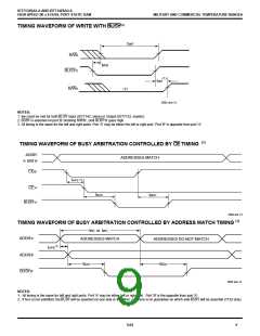
TABLE II — ADDRESS BUSY ARBITRATION
The use of busy logic is not required or desirable for all
applications. In some cases it may be useful to logically OR
the busy outputs together and use any busy indication as an
interrupt source to flag the event of an illegal or illogical
operation. If the write inhibit function of busy logic is not
desirable, the busy logic can be disabled by placing the part
in slave mode with the M/S pin. Once in slave mode the
BUSYpin operates solely as a write inhibit input pin. Normal
operation can be programmed by tying the BUSY pins High.
If desired, unintended write operations can be prevented to
a port by tying the busy pin for that port low.
Inputs
Outputs
A0L-A10L
CER A0R-A10R BUSYL
(1)
(1)
CEL
X
BUSYR
Function
Normal
X
X
H
L
NO MATCH
MATCH
H
H
H
H
H
Normal
X
MATCH
H
H
Normal
Write Inhibit(3)
L
MATCH
(2)
(2)
2654 tbl 13
NOTES:
1. Pins BUSYL and BUSYR are both outputs for IDT7130 (master). Both are
inputs for IDT7140 (slave). BUSYX outputs on the IDT7130 are open
drain,notpush-pulloutputs. Onslavesthe BUSYX inputinternallyinhibits
writes.
2. 'L' if the inputs to the opposite port were stable prior to the address and
enable inputs of this port. 'H' if the inputs to the opposite port became
stable after the address and enable inputs of this port. If tAPS is not met,
eitherBUSYL orBUSYR = Low will result. BUSYL andBUSYR outputs can
not be low simultaneously.
The busy outputs on the IDT7132/IDT7142 RAM in master
mode, are pull-up type outputs and do not require pull up
resistors to operate. If these RAMs are being expanded in
depth, then the busy indication for the resulting array re-
quires the use of an external AND gate.
3. Writes to the left port are internally ignored when BUSYL outputs are
driving Low regardless of actual logic level on the pin. Writes to the right
port are internally ignored when BUSYR outputs are driving Low regard-
less of actual logic level on the pin.
6.02
10

 IDT [ INTEGRATED DEVICE TECHNOLOGY ]