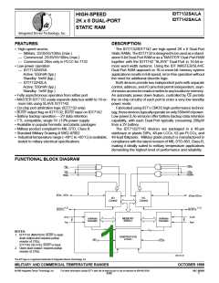
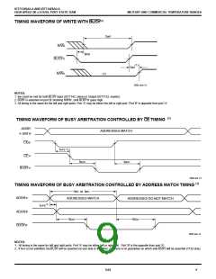
IDT7132SA/LA AND IDT7142SA/LA
HIGH-SPEED 2K x 8 DUAL-PORT STATIC RAM
MILITARY AND COMMERCIAL TEMPERATURE RANGES
lDT7132LA/IDT7142LA
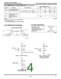
DATA RETENTION CHARACTERISTICS (LA Version Only)
Symbol
Parameter
Test Conditions
Min.
Typ.
Max.
Unit
VDR
VCC for Data Retention
Data Retention Current
2.0
—
—
—
V
ICCDR
VCC = 2.0V, CE ≥ VCC -0.2V
Mil.
100
100
4000
1500
µA
µA
VIN ≥ VCC -0.2V or VIN ≤ 0.2V Com’l.
—
(3)
tCDR
Chip Deselect to Data
Retention Time
0
—
—
—
—
ns
(3)
(2)
tR
Operation Recovery
Time
tRC
ns
2692 tbl 06
NOTES:
1. VCC = 2V, TA = +25°C, and is not production tested.
2. tRC = Read Cycle Time
3. This parameter is guaranteed but not production tested.
AC TEST CONDITIONS
DATA RETENTION WAVEFORM
Input Pulse Levels
GND TO 3.0V
5ns
DATA RETENTION MODE
Input Rise/Fall Times
Input Timing Reference Levels
Output Reference Levels
Output Load
1.5V
1.5V
VCC
V
DR
≥
2.0V
Figures 1, 2, and 3
4.5V
4.5V
2692 tbl 07
tCDR
t
R
VDR
CE
V
IH
V
IH
2692 drw 05
5V
5V
1250Ω
1250Ω
DATA OUT
775Ω
DATA OUT
30pF*
775Ω
5pF*
100pF for 55 and 100ns versions
2692 drw 06
Figure 1. AC Output Test Load
Figure 2. Output Test Load
(for tHZ, tLZ, tWZ, and tOW)
* Including scope and jig
5V
270Ω
BUSY or INT
30pF*
100pF for 55 and 100ns versions
Figure 3. BUSY and INT
AC Output Test Load
6.02
4

 IDT [ INTEGRATED DEVICE TECHNOLOGY ]