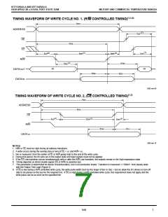
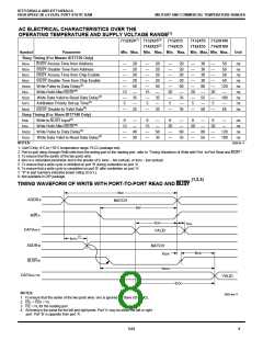
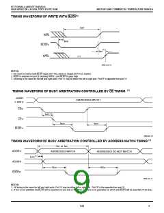
IDT7132SA/LA AND IDT7142SA/LA
HIGH-SPEED 2K x 8 DUAL-PORT STATIC RAM
MILITARY AND COMMERCIAL TEMPERATURE RANGES
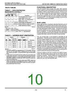
WIDTH EXPANSION WITH BUSY LOGIC
MASTER/SLAVE ARRAYS
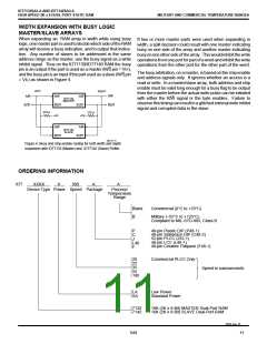
When expanding an RAM array in width while using busy
logic, onemasterpartisusedtodecidewhichsideoftheRAM
array will receive a busy indication, and to output that indica-
tion. Any number of slaves to be addressed in the same
address range as the master, use the busy signal as a write
inhibit signal. Thus on the IDT7130/IDT7140 RAM the busy
pin is an output if the part is used as a master (M/Spin = VIH),
and the busy pin is an input if the part used as a slave (M/Spin
= VIL) as shown in Figure 4.
If two or more master parts were used when expanding in
width, a split decision could result with one master indicating
busy on one side of the array and another master indicating
busyononeothersideofthearray. Thiswouldinhibitthewrite
operations from one port for part of a word and inhibit the write
operations from the other port for the other part of the word.
The busy arbitration, on a master, is based on the chip enable
and address signals only. It ignores whether an access is a
read or write. In a master/slave array, both address and chip
enable must be valid long enough for a busy flag to be output
from the master before the actual write pulse can be initiated
with either the R/W signal or the byte enables. Failure to
observe this timing can result in a glitched internal write inhibit
signal and corrupted data in the slave.
LEFT
RIGHT
R/W
R/W
R/W
R/W
IDT7132
MASTER
BUSY
BUSY
BUSY
BUSY
270 Ω
270 Ω
+5V
+5V
R/W
R/W
IDT7142
IDT714(21)
SLAVE
SLAVE
BUSY
BUSY
2692 drw 15
Figure 4. Busy and chip enable routing for both width and depth
expansion with IDT7132 (Master) and IDT7142 (Slave) RAMs.
ORDERING INFORMATION
IDT
XXXX
A
999
A
A
Device Type Power Speed Package
Process/
Temperature
Range
Blank
Commercial (0°C to +70°C)
B
Military (–55°C to +125°C)
Compliant to MIL-STD-883, Class B
P
48-pin Plastic DIP (P48-1)
48-pin Sidebraze DIP (C48-2)
52-pin PLCC (J52-1)
C
J
L48
F
48-pin LCC (L48-1)
48-pin Ceramic Flatpack (F48-1)
20
25
35
55
100
Commercial PLCC Only
Speed in nanoseconds
LA
SA
Low Power
Standard Power
7132
7142
16K (2K x 8-Bit) MASTER Dual-Port RAM
16K (2K x 8-Bit) SLAVE Dual-Port RAM
2692 drw 16
6.02
11

 IDT [ INTEGRATED DEVICE TECHNOLOGY ]