IDT7132SA/LA AND IDT7142SA/LA
HIGH-SPEED 2K x 8 DUAL-PORT STATIC RAM
MILITARY AND COMMERCIAL TEMPERATURE RANGES
(3)
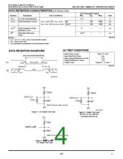
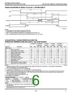
TIMING WAVEFORM OF READ CYCLE NO. 2, EITHER SIDE
tACE
CE
OE
AOE(4)
t
HZ(2)
t
(2)
HZ
(1)
t
t
LZ
VALID DATA
DATAOUT
t
LZ(1)
(4)
PD
t
t
PU
ICC
CURRENT
50%
50%
I
SS
2692 drw 08
NOTES:
1. Timing depends on which signal is asserted last, OE or CE.
2. Timing depends on which signal is deaserted first, OE or CE.
3. R/W = VIH, and the address is valid prior to or coincidental with CE transition Low.
4. Start of valid data depends on which timing becomes effective last tAOE, tACE, tAA, and tBDD.
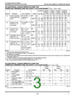
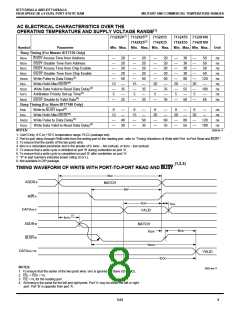
AC ELECTRICAL CHARACTERISTICS OVER THE
OPERATING TEMPERATURE AND SUPPLY VOLTAGE RANGE(5)
(2)
(6)
7132X20
7132X25
7132X35
7132X55
7142X55
7132X100
7142X100
(6)
7142X25
7142X35
Symbol
Parameter
Min. Max. Min. Max. Min. Max. Min. Max. Min. Max. Unit
Write Cycle
tWC
tEW
tAW
tAS
Write Cycle Time(3)
20
15
15
0
15
0
10
—
0
—
0
—
—
—
—
—
—
—
10
—
10
—
25
20
20
0
15
0
12
—
0
—
0
—
—
—
—
—
—
—
10
—
10
—
35
30
30
0
25
0
15
—
0
—
0
—
—
—
—
—
—
—
15
—
15
—
55
40
40
0
30
0
20
—
0
—
0
—
—
—
—
—
—
—
25
—
30
—
100
90
90
0
55
0
40
—
0
—
0
—
—
—
—
—
—
—
40
—
40
—
ns
ns
ns
ns
ns
ns
ns
ns
ns
ns
ns
Chip Enable to End of Write
Address Valid to End of Write
Address Set-up Time
tWP
tWR
tDW
tHZ
Write Pulse Width(4)
Write Recovery Time
Data Valid to End of Write
Output High Z Time(1)
tDH
tWZ
tOW
Data Hold Time
Write Enabled to Output in High Z(1)
Output Active From End of Write(1)
NOTES:
2692 tbl 09
1. Transition is measured ±500mV from Low or High-impedance voltage with Output Test Load (Figure 2). This parameter is guaranteed by
device characterization but is not production tested.
2. 0°C to +70°C temperature range only, PLCC package only.
3. For Master/Slave combination, tWC = tBAA + tWP, since R/W = VIL must occur after tBAA.
4. If OE is low during a R/W controlled write cycle, the write pulse width must be the larger of tWP or (tWZ + tDW) to allow the I/O drivers to turn off
data to be placed on the bus for the required tDW. If OE is High during a R/W controlled write cycle, this requirement does not apply and the
write pulse can be as short as the specified tWP.
5. “X” in part numbers indicates power rating (SA or LA).
6. Not available in DIP packages.
CAPACITANCE(1) (TA = +25°C,f = 1.0MHz)
Symbol
Parameter
Conditions(2) Max. Unit
CIN
Input Capacitance
Output Capacitance
VIN = 3dV
VIN = 3dV
11
11
pF
pF
COUT
NOTES:
2692 tbl 10
1. This parameter is determined by device characterization but is not
production tested.
2. 3dV represents the interpolated capacitance when the input and output
signals switch from 0V to 3V or from 3V to 0V.
6.02
6

 IDT [ INTEGRATED DEVICE TECHNOLOGY ]