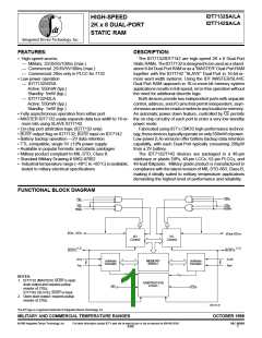
IDT7132SA/LA AND IDT7142SA/LA
HIGH-SPEED 2K x 8 DUAL-PORT STATIC RAM
MILITARY AND COMMERCIAL TEMPERATURE RANGES
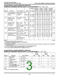
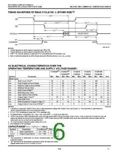
AC ELECTRICAL CHARACTERISTICS OVER THE
OPERATING TEMPERATURE AND SUPPLY VOLTAGE RANGE(3)
7132X20(2) 7132X25(5) 7132X35
7142X25(5) 7142X35
7132X55
7142X55
7132X100
7142X100
Symbol
Parameter
Min. Max. Min. Max. Min. Max. Min. Max. Min. Max. Unit
Read Cycle
tRC
tAA
Read Cycle Time
Address Access Time
Chip Enable Access Time
Output Enable Access Time
Output Hold From Address Change
Output Low-Z Time(1,4)
Output High-Z Time(1,4)
Chip Enable to Power Up Time(4)
Chip Disable to Power Down Time(4)
20
—
—
—
20
20
11
—
—
10
—
20
25
—
—
—
3
—
25
25
12
—
—
10
—
25
35
—
—
—
3
—
35
35
20
—
—
15
—
35
55
—
—
—
3
—
55
55
25
—
—
25
—
50
100
—
—
—
10
5
—
ns
100 ns
100 ns
tACE
tAOE
tOH
tLZ
40
—
—
40
—
50
ns
ns
3
0
0
0
5
ns
tHZ
tPU
—
0
—
0
—
0
—
0
—
0
ns
ns
tPD
—
—
—
—
—
ns
NOTES:
2689 tbl 08
1. Transition is measured ±500mV from Low or High-impedance voltage Output Test Load (Figure 2).
2. Com'l Only, 0°C to +70°C temperature range. PLCC package only.
3. “X” in part numbers indicates power rating (SA or LA).
4. This parameter is guaranteed by device characterization, but is not production tested.
5. Not available in DIP packages.
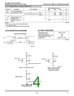
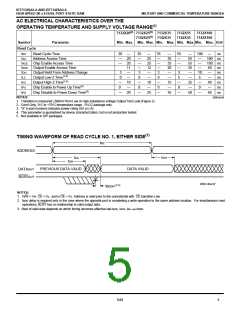
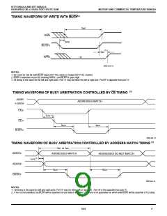
TIMING WAVEFORM OF READ CYCLE NO. 1, EITHER SIDE(1)
t
RC
ADDRESS
t
AA
tOH
t
OH
PREVIOUS DATA VALID
DATA VALID
DATAOUT
BUSYOUT
2692 drw 07
(2,3)
t
BDDH
NOTES:
1. R/W = VIH, CE = VIL, and is OE = VIL. Address is valid prior to the coincidental with CE transition Low.
2. tBDD delay is required only in the case where the opposite port is completing a write operation to the same address location. For simultaneous read
operations, BUSY has no relationship to valid output data.
3. Start of valid data depends on which timing becomes effective last tAOE, tACE, tAA, and tBDD.
6.02
5

 IDT [ INTEGRATED DEVICE TECHNOLOGY ]