IDT7132SA/LA AND IDT7142SA/LA
HIGH-SPEED 2K x 8 DUAL-PORT STATIC RAM
MILITARY AND COMMERCIAL TEMPERATURE RANGES
PIN CONFIGURATIONS (1,2)
INDEX
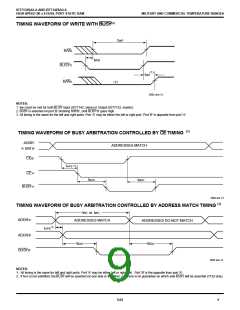
CE
R/W
BUSY
L
L
L
10L
1
48
47 CE
46 R/W
45 BUSY
44
43 OE
V
CC
R
2
3
R
6
5
4
3
2
48 47 46 45 44 43
1
A
4
R
A
A
A
A
A
A
A
0R
1R
2R
3R
4R
5R
6R
A
1L
2L
3L
4L
5L
6L
7L
8L
9L
7
42
41
40
39
38
37
36
35
34
33
32
31
OE
L
5
A
10R
R
0R
A
A
A
A
A
A
A
A
8
A
A
A
A
A
A
A
A
A
A
0L
1L
2L
3L
4L
5L
6L
7L
8L
9L
6
9
7
42
41
40
39
38
37
36
35
34
33
A
A
A
A
A
A
A
A
A
A
10
11
12
13
14
15
16
17
18
8
1R
2R
3R
4R
5R
6R
7R
8R
9R
IDT7132/42
L48-1
&
IDT7132/
7142
9
10
11
12
13
14
15
16
17
18
F48-1
P48-1
&
C48-2
48-PIN LCC/ FLATPACK
TOP VIEW (3)
A
A
7R
8R
A
9R
I/O0L
I/O1L
I/O2L
DIP
TOP
I/O0L
I/O1L
I/O2L
I/O3L 19
I/O4L 20
I/O5L 21
I/O6L 22
I/O7L 23
GND 24
I/O7R
I/O6R
32 I/O7R
31 I/O6R
30 I/O5R
29 I/O4R
28 I/O3R
27 I/O2R
26 I/O1R
25 I/O0R
VIEW (3)
19 20 21 22 23 24 25 26 27 28 29 30
2692 drw 03
INDEX
2692 drw 02
NOTES:
7
6
5
4
3
2
52 51 50 49 48 47
1. All Vcc pins must be connected to the power supply.
2. All GND pins must be connected to the ground supply.
3. This text does not indicate orientation of the actual part-marking.
1
8
46
A
1L
2L
3L
4L
5L
6L
7L
8L
9L
OER
9
45
44
43
42
41
40
39
38
37
36
35
34
A
A
A
A
A
A
A
A
A
A
A
A
A
A
A
A
A
A
0R
10
11
12
13
14
15
16
17
18
19
20
1R
2R
3R
4R
5R
6R
7R
8R
9R
ABSOLUTE MAXIMUM RATINGS(1)
Symbol
IDT7132/42
J52-1
Rating
Commercial
Military
Unit
52-PIN PLCC
TOP VIEW (3)
(2)
VTERM
Terminal Voltage -0.5 to +7.0 -0.5 to +7.0
with Respect to
GND
V
I/O0L
I/O1L
I/O2L
I/O3L
TA
Operating
Temperature
0 to +70
-55 to +125
°C
°C
°C
N/C
TBIAS
TSTG
Temperature
Under Bias
-55 to +125 -65 to +135
-55 to +125 -65 to +150
I/O7R
21 22 23 24 25 26 27 28 29 30 31 32 33
Storage
2692 drw 04
Temperature
IOUT
DC Output
Current
50
50
mA
NOTES:
2692 tbl 01
NOTES:
1. All Vcc pins must be connected to the power supply.
2. All GND pins must be connected to the ground supply.
3. This text does not indicate orientation of the actual part-marking.
1. StressesgreaterthanthoselistedunderABSOLUTEMAXIMUMRATINGS
may cause permanent damage to the device. This is a stress rating only
and functional operation of the device at these or any other conditions
above those indicated in the operational sections of the specification is not
implied. Exposure to absolute maximum rating conditions for extended
periods may affect reliability.
2. VTERM must not exceed Vcc + 0.5V for more than 25% of the cycle time or
10ns maximum, and is limited to < 20mA for the period of VTERM > Vcc +
0.5V.
RECOMMENDED
DC OPERATING CONDITIONS
Symbol
Parameter
Min. Typ. Max. Unit
VCC
Supply Voltage
Supply Voltage
4.5
0
5.0
0
5.5
V
V
RECOMMENDED OPERATING
TEMPERATURE AND SUPPLY VOLTAGE
Ambient
GND
0
VIH
VIL
Input High Voltage
Input Low Voltage
2.2
-0.5(1)
—
—
6.0(2)
0.8
V
V
Grade
Military
Commercial
Temperature
-55°C to +125°C
0°C to +70°C
GND
VCC
2692 tbl 03
NOTES:
0V
5.0V ± 10%
5.0V ± 10%
1. VIL (min.) = -1.5V for pulse width less than 10ns.
2. VTERM must not exceed Vcc + 0.5V.
0V
2692 tbl 02
6.02
2

 IDT [ INTEGRATED DEVICE TECHNOLOGY ]