IDT70V5388/78
3.3V 64/32K x 18 Synchronous FourPort™ Static RAM
Industrial and Commercial Temperature Ranges
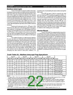
Address Counter Control Operations
EachportontheIDT70V5388/78isequippedwith
an internal address counter, to ease the process of
burstingdataintooroutofthedevice.TruthTableIIdepicts
the specific operation of the counter functions, to include
theorderofpriorityamongthesignals.Allcountercontrols
areindependentofchipenables.Thedevicesupportsthe
ability to load a new address value on each access, or to
loadanaddressvalueonagivenclockcycleviatheCNTLD
controlandthenallowthecountertoincreasethatvalueby
preset increments on each successive clock via the
CNTINC control (see also the Counter Mask Operations
section that follows). The counter can be suspended on
any clock cycle by disabling the CNTINC, and it can be
reset to zero on any clock cycle by asserting the CNTRST
control.CNTRST onlyaffectstheaddressvaluestoredinthe
counter: it has no effect on the counter mask register.
Whenthecounterreachesthemaximumvaluein
thearray(i.e.,addressFFFFhforIDT70V5388andaddress
7FFFh for IDT70V5378) or it reaches the highest value
permitted by the Counter Mask Register, it then ‘wraps
around’tothebeginningofthearray.WhenAddressMinis
reached via counter increment (i.e., not as a result of an
externaladdressload),thentheCNTINT signalforthatport
isdrivenlowforoneclockcycle,automaticallyresettingon
the next cycle.
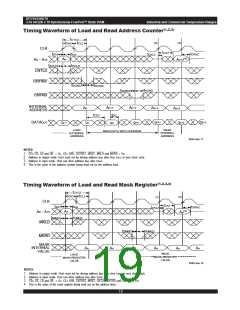
When the CNTRD control is asserted, the
IDT70V5388/78willoutputthecurrentaddressstoredinthe
internalcounterforthatportasnotedintheLoadandRead
AddressCountertimingwaveformonpage19.Theaddress
will be output on the address lines. During this output, the
data I/Os will be driven in accordance with the settings of
the chip enables, byte enables, and the output enable on
that port: the device does not automatically tri-state these
pins during the address readback operation.
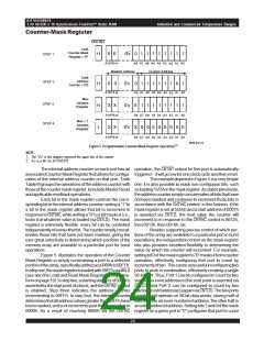
CNTRD
MKRD
Read Back
Register
Addr.
Read
Back
MKLD
Memory
Array
Mask
Register
Address
(I/O)
Counter/
Address
Register
CNTLD
CNTINC
CNTRST
,
CLK
5649 drw 22
Figure 4. Logic Block Diagram for Read Back Operations
23
6.42

 IDT [ INTEGRATED DEVICE TECHNOLOGY ]