IDT70V5388/78
3.3V 64/32K x 18 Synchronous FourPort™ Static RAM
Industrial and Commercial Temperature Ranges
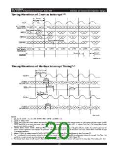
MailboxInterrupts
possible to do so by disabling the byte enables during that
write cycle.
TheIDT70V5388/78supportsmailboxinterrupts,
facilitatingcommunicationamongthedevicesattachedto
each port. If the user chooses the interrupt function, then
each of the upper four address locations in the memory
arrayareassignedasamailboxforoneoftheports:FFFFh
(7FFFh for IDT70V5378) is the mailbox for Port 1, FFFEh
(7FFEh for IDT70V5378) is the mailbox for Port 2, FFFDh
(7FFDh for IDT70V5378) is the mailbox for Port 3, and
FFFCh (7FFCh for IDT70V5378) is the mailbox for Port 4.
TruthTableIIIdetailstheoperationofthemailboxinterrupt
functions.
Once INT has gone LOW for a specific port, that
port can reset the INT by reading its assigned mailbox. In
the case of Port 1, it would clear its INT signal by reading
FFFFh(7FFFhforIDT70V5378).Asstatedpreviously,the
interrupt operation executes based on the state of the
address pins, the chip enables, and the R/W pin: it is
possible to clear the interrupt by asserting a read to the
appropriatelocationwhilekeepingtheoutputenable(OE)or
the byte enables deasserted, and so avoid having to drive
data on the I/O bus. The INT is reset, or goes HIGH again,
in relation to the reading port’s clock signal.
A given port’s interrupt is set (i.e., INT goes LOW)
whenever any other port on the device writes to the given
port’saddress.Forexample,Port1’sINTwillgoLOWifPort
2,Port3,orPort4writetoFFFFh(7FFFhforIDT70V5378).
The INT will go LOW in relation to the clock on the writing
port (see also the Mailbox Interrupt Timing waveform on
page 20). If a port writes to its own mailbox, no interrupt is
generated.
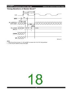
MasterReset
TheIDT70V5388/78isequippedwithanasynchro-
nousMasterResetinput,whichcanbeassertedindepen-
dentlyofallclockinputsandwilltakeeffectpertheMaster
Resettimingwaveformonpage18.TheMasterResetsets
theinternalvalueofalladdresscounterstozero, andsets
the counter mask register on each port to all ones (i.e.,
completelyunmasked).Italsoresetsallmailboxinterrupts
and counter interrupts to HIGH (i.e., non-asserted) and
sets all registered control signals to a deselected state. A
MasterResetoperationmustbeperformedafterpower-up,
inordertoinitializethevariousregistersonthedevicetoa
knownstate.MasterResetwillresetthedevice.ForJTAG
andMBISTresetpleaserefertotheJTAGSectiononpage
25.
The mailbox location is a valid memory address:
the user can store an 18-bit data word at that location for
retrievalbythetargetport.Intheeventthattwoormoreports
attempt to set an interrupt to the same port at the same
time, theinterruptsignalwillgoLOW, butthedataactually
stored at that location will be indeterminate. The actual
interrupt is generated as a result of evaluating the state of
the address pins, the chip enables, and the R/W pin: if the
user wishes to set an interrupt to a specific port without
changing the data stored in that port’s mailbox, it is
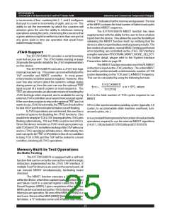
Truth Table III—Mailbox Interrupt Flag Operations
Port 1(1,2)
Port 2(1,2)
Port 3(1,2)
Port 4(1,2)
(4)
(4)
(4)
(4)
CE
X
L
INT
L
CE
L
INT
X
CE
L
INT
X
CE
L
INT
X
R/W
A
15-
A
0
R/W
L
A
15-
A
0
R/W
L
A
15-
A
0
R/W
L
A
15-
A
0
Function
X
X
FFFF
X
FFFF
X
FFFF
X
Set Port 1 INT Flag(3)
Reset Port 1 INT Flag
Set Port 2 INT Flag(3)
Reset Port 2 INT Flag
Set Port 3 INT Flag(3)
Reset Port 3 INT Flag
Set Port 4 INT Flag(3)
Reset Port 4 INT Flag
H
FFFF
FFFE
X
H
X
X
X
X
L
X
X
X
L
X
X
X
L
X
L
L
X
X
L
L
FFFE
X
X
L
FFFE
X
X
X
X
L
X
H
L
FFFE
FFFD
X
H
X
X
X
X
L
X
X
X
L
X
L
FFFD
X
X
L
X
X
L
L
FFFD
X
X
X
X
L
X
X
X
L
X
H
L
FFFD
FFFC
X
H
X
X
X
X
L
X
L
X
FFFC
X
X
L
FFFC
X
X
L
X
X
L
X
X
X
X
X
X
X
X
H
FFFC
H
5649 tbl 14
NOTES:
1. The status of OE is a "Don't Care" for the interrupt logic circuitry. If it is desirable to reset the interrupt flag on a given port while keeping the I/O bus in a tri-state
condition, then this can be accomplished by setting OE = VIH while the read access is asserted to the appropriate address location.
2. The status of the LB and UB controls are "Don't Care" for the interrupt circuitry. If it is desirable to set the interrupt flag to a specific port without overwriting the
data value already stored at the mailbox location, then this can be accomplished by setting LB = UB = VIH during the write access for that specific mailbox.
Similarly, if it desirable to reset the interrupt flag on a given port while keeping the I/O bus in a tri-state condition, then this can be accomplished by setting LB
= UB = VIH while the read access is asserted to the appropriate address location.
3. The interrupt to a specific port can be set by any one of the other three ports. The appropriate control states for the other three ports are depicted above. In the
event that two or more ports attempt to set the same interrupt flag simultaneously via a valid data write, the data stored at the mailbox location will be
indeterminate.
4. A15 is a NC for IDT70V5378, therefore Mailbox Interrupt Addresses are 7FFF, 7FFE, 7FFD and 7FFC. Address comparison will be for A0 - A14.
22

 IDT [ INTEGRATED DEVICE TECHNOLOGY ]