IDT70V5388/78
3.3V 64/32K x 18 Synchronous FourPort™ Static RAM
Industrial and Commercial Temperature Ranges
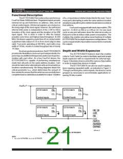
FunctionalDescription
TheIDT70V5388/78providesatruesynchronous
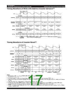
oftCCS mayproduceindeterminatedatafortheread.Twoor
more ports attempting to write the same address location
simultaneouslywillresultinindeterminatedatarecordedat
that address.
FourPort Static RAM interface. Registered inputs provide
minimal set-up and hold times on address, data, and all
critical control inputs. All internal registers are clocked on
therisingedgeoftheclocksignal, however, theself-timed
internal write pulse is independent of the LOW to HIGH
transition of the clock signal and the duration of the R/W
input signal. This is done in order to offer the fastest
possible cycle times and highest data throughput. At 200
MHz,thedevicesupportsacycletimeof5ns,andprovides
a pipelined data output of 3.0 ns from clock edge to data
valid. Four ports operating at 200 MHz, each with a bus
width of 18 bits, results in a data throughput rate of nearly
14 Gbps.
Eachportisequippedwithdualchipenables, CE0
and CE1. A HIGH on CE0 or a LOW on CE1 for one clock
cycle on any port will power down the internal circuitry on
thatportinordertoreducestaticpowerconsumption. The
multiplechipenablesalsoalloweasierbankingofmultiple
IDT70V5388/78sfordepthexpansionconfigurations.One
cycleisrequiredwithchipenablesreassertedtoreactivate
the outputs.
Depth and Width Expansion
Asatruesynchronousdevice,theIDT70V5388/78
providestheflexibilitytoclockeachportindependently:the
portsmayrunatdifferentfrequenciesand/oroutofsynchro-
nization with each other. As a true FourPort device, the
IDT70V5388/78 is capable of performing simultaneous
reads from all ports on the same address location. Care
shouldbetakenwhenattemptingtowriteandreadaddress
locations simultaneously: the timing diagrams depict the
critical parameter tCCS, which determines the amount of
timeneededtoensurethatthewritehassuccessfullybeen
completedandsovaliddataisavailableforoutput.Violation
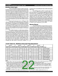
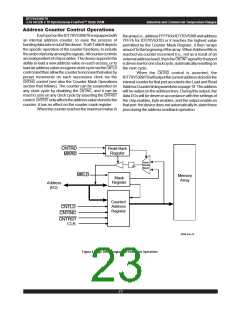
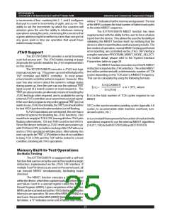
The IDT70V5388/78 features dual chip enables
(refertoTruthTableI)inordertofacilitaterapidandsimple
depth expansion with no requirements for external logic.
Figure 4 illustrateshowtocontrolthevariouschipenables
in order to expand two devices in depth.
The IDT70V5388/78 can also be used in applica-
tions requiring expanded width, as indicated in Figure 3.
Throughcombiningthecontrolsignals,thedevicescanbe
grouped as necessary to accommodate applications re-
quiring36-bitsorwider.
(1)
A16/A15
IDT70V5388/78
IDT70V5388/78
CE0
CE0
CE1
CE1
VDD
VDD
Control Inputs
Control Inputs
IDT70V5388/78
IDT70V5388/78
CE1
CE1
UB, LB
R/W,
OE,
CE0
CE0
Control Inputs
Control Inputs
CLK,
CNTLD,
CNTRST,
CNTINC
5649 drw 21
Figure 3. Depth and Width Expansion with IDT70V5388/78
NOTE:
1. A16 is for IDT70V5388, A15 is for IDT70V5378.
21
6.42

 IDT [ INTEGRATED DEVICE TECHNOLOGY ]