IDT70V5388/78
3.3V 64/32K x 18 Synchronous FourPort™ Static RAM
Industrial and Commercial Temperature Ranges
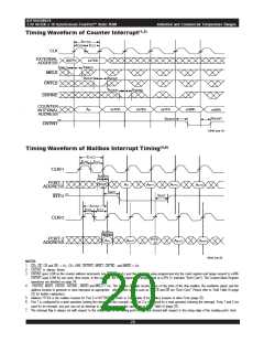
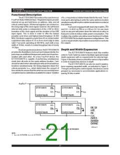
Timing Waveform of Counter Interrupt(1,3)
t
CYC2
t
CH2 CL2
t
CLK
EXTERNAL
ADDRESS
007Fh
xx7Dh
tHMLD
tSMLD
MKLD
tSCLD
tHCLD
CNTLD
tSCINC
tHCINC
CNTINC
COUNTER
INTERNAL
ADDRESS
xx7Eh
xx7Fh
xx00h
xx7Dh
A
n
xx00h
,
tRCINT
tSCINT
(2)
CNTINT
5649 drw 19
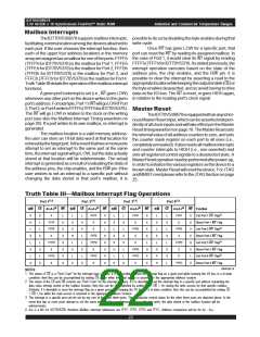
Timing Waveform of Mailbox Interrupt Timing(4,6)
t
CYC2
t
CH2 CL2
t
CLKP1
tSA tHA
PORT-1
ADDRESS
FFFE
An
An+1
An+2
An+3
(5)
tSINT
INTP2 (7)
tRINT
t
CYC2
t
CH2 CL2
t
CLKP2
tSA tHA
PORT-2
ADDRESS
,
FFFE
Am
Am+1
Am+3
A
m+4
(5)
5649 drw 20
NOTES:
1. CE0, OE, LB and UB = VIL; CE1, R/W, CNTRST, MRST, CNTRD and MKRD = VIH.
2. CNTINT is always driven.
3. CNTINT goes LOW as the counter address increments (via CNTINC = VIL) past the maximum value programmed into the mask register and 'wraps around' to xx00h
CNTINT stays LOW for one cycle, then resets. In this example, the mask register was programmed at xx7Fh ('x' indicates "Don't Care"). The Counter Mask Register
operations are detailed on page 24.
4. CNTRST, MRST, CNTRD CNTINC , MKRD and MKLD = VIH. The mailbox interrupt circuitry relies on the state of the chip enables, the read/write signal, and the
address location to generate or clear interrupts as appropriate - other control signals such as OE, LB and UB are "Don't Care". Please refer to Truth Table III (page
22) for further explanation.
5. Address FFFEh is the mailbox location for Port 2 of IDT70V5388. Refer to Truth Table III for mailbox location of other Ports (page 22).
6. Port 1 is configured for a write operation (setting the interrupt) in this example, and Port 2 is configured for a read operation (clearing the interrupt). Ports 1 and 2 are
used for an example: any port can set an interrupt to any other port per the operations in Truth Table III (page 22).
7. The interrupt flag is always set with respect to the rising edge of the writing port's clock, and cleared with respect to the rising edge of the reading port's clock.
20

 IDT [ INTEGRATED DEVICE TECHNOLOGY ]