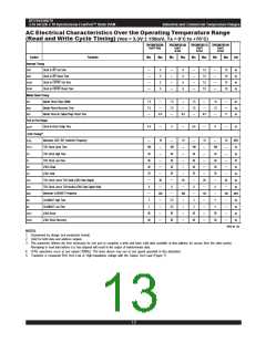
IDT70V5388/78
3.3V 64/32K x 18 Synchronous FourPort™ Static RAM
Industrial and Commercial Temperature Ranges
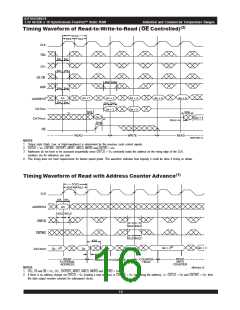
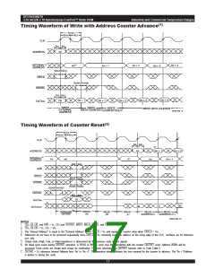
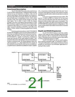
Timing Waveform of Write with Address Counter Advance(1)
t
CYC2
tCH2
tCL2
CLK
tSA
tHA
An
ADDRESS
INTERNAL(3)
ADDRESS
An(7)
An + 1
An + 3
An + 4
An + 2
tSCLD tHCLD
CNTLD
tSCINC tHCINC
CNTINC
tSD tHD
Dn + 4
Dn + 1
Dn + 3
Dn
Dn + 1
Dn + 2
DATAIN
WRITE
EXTERNAL
ADDRESS
WRITE
WITH COUNTER
WRITE
COUNTER HOLD
WRITE WITH COUNTER
5649 drw 14
Timing Waveform of Counter Reset(2)
t
CYC2
tCH2
tCL2
CLK
tSA
tHA
(4)
An + 2
An
An + 1
ADDRESS
INTERNAL(3)
ADDRESS
Ax
A1
A0
An
An + 1
tSW tHW
R/
W
CNTLD
tSCLD
tHCLD
CNTINC
tSCINC tHCINC
tSCRST tHCRST
CNTRST
tSD
tHD
D0
DATAIN
(5)
Q1
Qn
Q0
DATAOUT
EXECUTE(6)
CNTRST
WRITE
READ
READ
READ
A0
READ
A1
A
0
ADDRESS n ADDRESS n+1
5649 drw 15
NOTES:
1. CE0, LB, UB, and R/W = VIL; CE1 and CNTRST, MRST, MKLD, MKRD, and CNTRD = vIH.
CE0, LB, UB = VIL; CE1 = VIH.
2.
3. The "Internal Address" is equal to the "External Address" when CNTLD = VIL and equals the counter value when CNTLD = VIH.
4. Addresses do not have to be accessed sequentially since CNTLD = VIL constantly loads the address on the rising edge of the CLK; numbers are for reference
use only.
5. Output state (High, Low, or High-impedance) is determined by the previous cycle control signals.
6. No dead cycle exists during CNTRST operation. A READ or WRITE cycle may be coincidental with the counter CNTRST cycle: Address 0000h will be
accessed. Extra cycles are shown here simply for clarification. For more information on CNTRST function refer to Truth Table II.
7. CNTINC = VIL advances Internal Address from ‘An’ to ‘An +1’. The transition shown indicates the time required for the counter to advance. The ‘An +1’Address
is written to during this cycle.
17
6.42

 IDT [ INTEGRATED DEVICE TECHNOLOGY ]