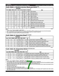
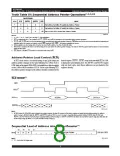
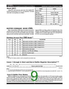
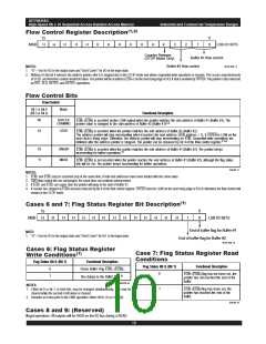
IDT70825S/L
High-Speed 8K x 16 Sequential Access Random Access Memory
Industrial and Commercial Temperature Ranges
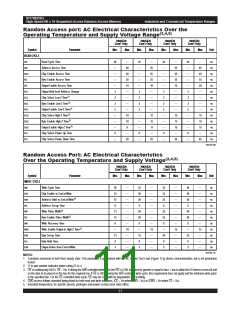
Random Access port: AC Electrical Characteristics Over the
Operating Temperature and Supply Voltage Range(2,4,5)
70825X20
70825X25
70825X35
70825X45
Com'l Only
Com'l Only
Com'l Only
Com'l Only
Symbol
Parameter
Min.
Max.
Min.
Max.
Min.
Max.
Min.
Max.
Unit
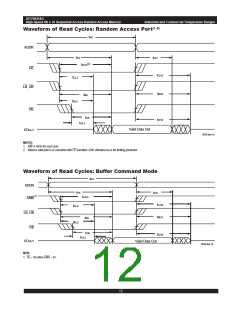
READ CYCLE
____
____
____
____
t
RC
AA
ACE
BE
OE
OH
CLZ
BLZ
OLZ
CHZ
BHZ
OHZ
PU
PD
Read Cycle Time
20
25
35
45
ns
ns
ns
ns
ns
ns
ns
ns
ns
ns
ns
ns
ns
____
____
____
____
t
Address Access Time
20
20
20
25
25
25
35
35
35
45
45
55
____
____
____
____
____
____
____
____
____
____
____
____
t
Chip Enable Access Time
Byte Enable Access Time
Output Enable Access Time
Output Hold from Address Change
Chip Select Low-Z Time(1)
Byte Enable Low-Z Time(1)
Output Enable Low-Z Time(1)
Chip Select High-Z Time(1)
Byte Enable High-Z Time(1)
Output Enable High-Z Time(1)
Chip Select Power Up Time
Chip Select Power Down Time
t
t
10
10
15
20
____
____
____
____
t
3
3
3
3
3
3
3
3
3
3
3
3
____
____
____
____
____
____
____
____
____
____
____
____
t
t
t
2
2
2
2
____
____
____
____
t
10
10
12
12
15
15
15
15
____
____
____
____
____
____
____
____
t
t
9
11
15
15
____
____
____
____
t
0
0
0
0
____
____
____
____
t
20
25
35
45
ns
3016 tbl 20a
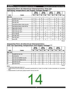
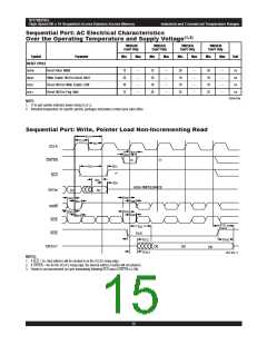
Random Access Port: AC Electrical Characteristics
Over the Operating Temperature and Supply Voltage(2,4,5)
70825X20
70825X25
70825X35
70825X45
Com'l Only
Com'l Only
Com'l Only
Com'l Only
Symbol
Parameter
Min.
Max.
Min.
Max.
Min.
Max.
Min.
Max.
Unit
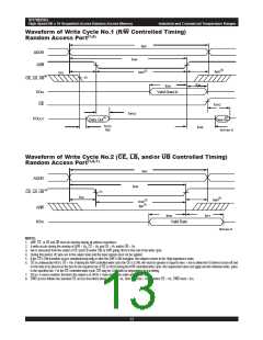
WRITE CYCLE
____
____
____
____
____
____
____
____
____
____
____
____
____
____
____
____
____
____
____
____
____
____
____
____
____
____
____
____
t
WC
CW
AW
AS
WP
BP
WR
WHZ
DW
DH
OW
Write Cycle Time
20
15
15
0
25
20
20
0
35
25
25
0
45
30
30
0
ns
ns
ns
ns
ns
ns
ns
ns
ns
ns
t
Chip Enable to End-of-Write
Address Valid to End-of-Write(3)
Address Set-up Time
t
t
t
Write Pulse Width(3)
13
15
20
20
25
25
30
30
t
Byte Enable Pulse Width(3)
Write Recovery Time
t
0
0
0
0
Write Enable Output in High-Z Time(1)
Data Set-up Time
10
12
15
15
____
____
____
____
t
____
____
____
____
t
13
0
15
0
20
0
25
0
____
____
____
____
____
____
____
____
t
Data Hold Time
t
Output Active from End-of-Write
3
3
3
3
ns
3016 tbl 21a
NOTES:
1. Transition measured at 0mV from steady state. This parameter is guaranteed with the AC Output Test Load (Figure 1) by device characterization, but is not production
tested.
2. 'X' in part number indicates power rating (S or L).
3. OE is continuously HIGH, OE = VIH. If during the R/W controlled write cycle the OE is LOW, tWP must be greater or equal to tWHZ + tDW to allow the I/O drivers to turn off and
on the data to be placed on the bus for the required tDW. If OE is HIGH during the R/W controlled write cycle, this requirement does not apply and the minimum write pulse
is the specified tWP. For the CE controlled write cycle, OE may be LOW with no degradation to tCW timing.
4. CMD access follows standard timing listed for both read and write accesses, (CE = VIH when CMD = VIL) or (CMD = VIH when CE = VIL).
5. Industrial temperature: for specific speeds, packages and powers contact your sales office.
6.42
11

 IDT [ INTEGRATED DEVICE TECHNOLOGY ]